Accelerating AES cipher on Zynq SoC-s10. Aug '14
Abstract
Cryptography is still pretty heavyweight task for embedded computers, but off-loading computationally expensive cryptography to programmable logic leverages the performance of ARM boards and allows higher utilization of network bandwidth available which otherwise might be lost due to encryption being the bottleneck.
With the introduction of 64-bit addressing support in ARMv8 there are finally ARM based servers popping up on the market 1 and it seems viable for such machines to have programmable logic for accelerating certain operations such as encrypting and decrypting HTTPS connections.
Current paper represents work carried out during summer semester as part of the Applied Embedded Systems Project at Technical University of Berlin conducted by Ahmed Elhossini. The team was composed of three students with open-source hacker background: Angelo Haller, Felix Kubicek and Lauri Võsandi.
Problem description
For the hardware we used ZYBO entry-level FPGA board which is available for around 150€ pricetag:
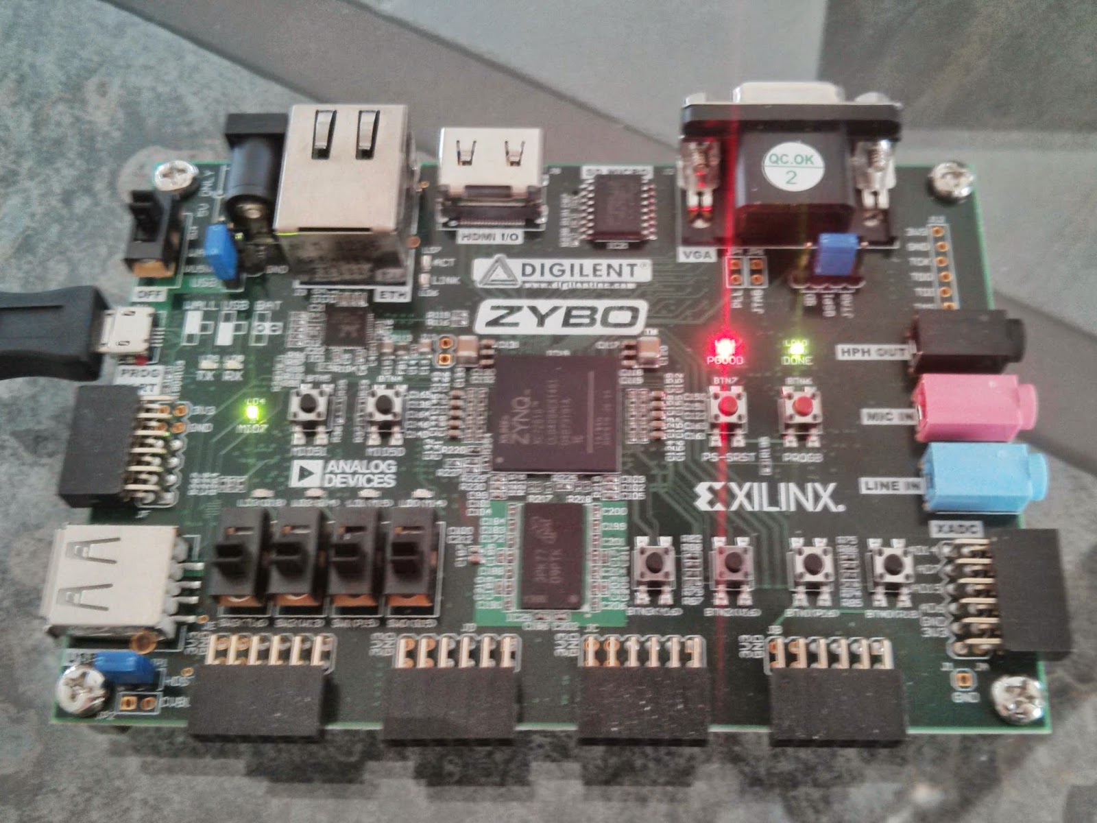
ZYBO is a feature-rich, ready-to-use, entry-level embedded software and digital circuit development platform
There is on-board gigabit network interface controller. In theory that should permit 100 MB/s throughput. This of course is limited by memory throughput, TCP/IP stack overhead and particular software architecure on either of the sides.
We did several experiments to determine different bottlenecks. First we discovered that copying to SD-card on ZYBO is a bad idea to measure bandwidth since SD-card writing speed drops usually below 10 MB/s depending on the speed class of the SD-card. Instead tmpfs was mounted to an arbitrary directory and files were copied there. To measure various ciphers we used OpenSSH and iterated Ciphers option over aes128-cbc, aes128-ctr and arcfour:
128-bit AES in cipher-block chaining mode: 11.9 MB/s
128-bit AES in counter mode: 11.9 MB/s
RC4 stream cipher: 17.3 MB/s
In addition we did a dummy test to measure throughput without encryption:
No encryption, using netcat: 59.3 MB/s
In all cases one of two ARM cores had 100% utilization since sshd and nc programs both are single-threaded. As can be easily seen the encrypted throughput is roughtly 6 times smaller than non-encrypted connection and we believe we can increase that at least twofold. Note that off-loading encryption/decryption to FPGA core also frees up ARM processor cycles.
Design
Our project is split into two components:
128-bit AES core
Kernel module compliant with Linux Crypto API
With this design we initially hoped to double AES throughput on the board.
AES core
As part of the project we implemented an AES core in VHDL which accelerates AES encryption, decryption, as well as key expansion. Detailed information about the AES standard can be found in the official document of the NIST 3. For the sake of simplicity the AES algorithm is implemented with a fixed block and key size (128-bit for both).
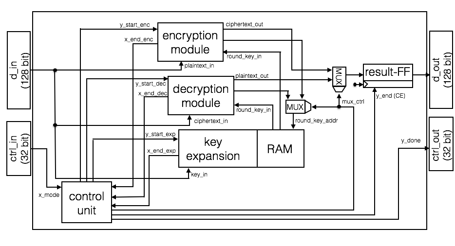
AES core internals
Figure above depicts the overall structure of the AES core. The core includes a control unit and additional subcomponents for encryption, decryption and key expansion, whereas each subcomponent has its own control unit as well. Conventionally, names of the signals leading to a control unit are starting with the letter “x”, whereas names of the output signals of a control unit are starting with the letter “y”. In the following subsections a brief overview of the encryption, decryption and key expansion module is given. Furthermore the basic behavior of the control unit is discussed. The following descriptions are related to figure above:
Key Expansion Module: Prior to the encryption/decryption a respective key of 128-bit width has to be set which is read out from the d_in register. For 128-bit AES (key and block size) there are 11 round keys, including the key itself for the initial round 3. The expansion module generates 10 round keys from the initial key using the AES key scheduling algorithm and stores the 11 keys in a dedicated RAM module.
Encryption Module: The encryption module performs the encryption of a 128-bit block read out from the d_in register. The whole encryption process is divided into rounds, in which various transformations are performed on the block. 128-bit AES (key and block size) comprises 10 rounds plus one initial round 3. Within each round, an associated round key is needed which is read out from the RAM of the key expansion module. After completion of all rounds the ciphertext is stored in the result flip-flop.
Decryption Module: The decryption module performs the decryption of a 128-bit block read out from the d_in register. The decryption process also comprises 10 rounds plus one initial round. The transformations within the rounds are the inverse of the transformations of encryption.
Control Unit
Following figure models the behavior of the control unit as control flow diagram. This structure of the diagram is inspired by the lecture “Grundlagen Digitaler Systeme” given by Dr.-Ing. Ralf Wollowski at Hasso-Plattner-Institut Potsdam in 2009 (Because the script is not publicly available it can’t be cited in the list of sources). The diagram specifies output signals only resulting from the internal state of the control unit (Moore characteristics) or additionally from the input signals (Mealy characteristics). The thick black bars within the diagram represent rising edges of the clock.
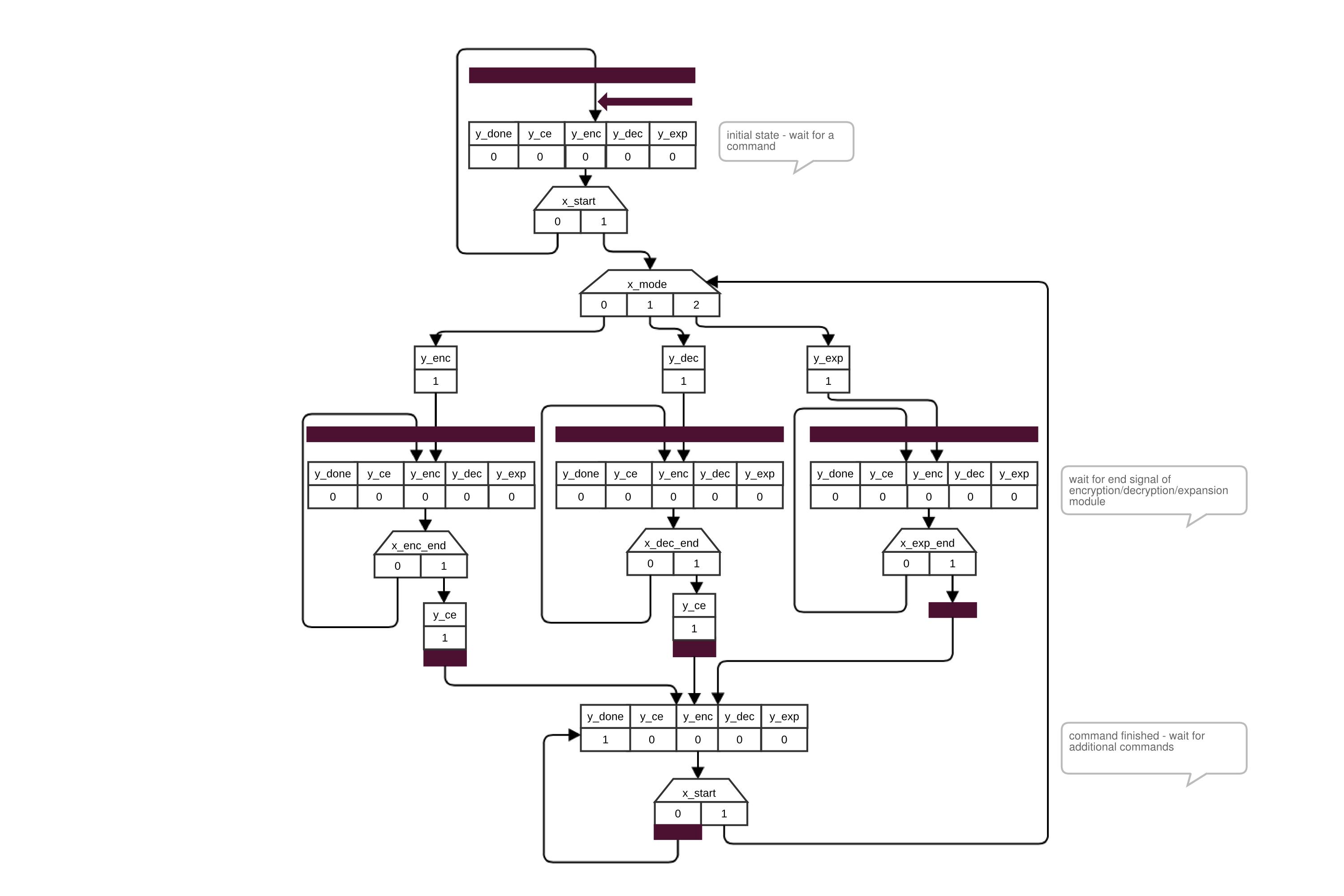
AES core control unit states
In the initial state the control unit waits for the start signal and for a specific mode. Both signals are read out from the ctrl_in register. If both are present the control unit immediately (Mealy characteristics) sets the start signal for either encryption, decryption or key expansion to logical one. Afterwards the control unit waits for the end signal indicating that the corresponding subcomponent is finished. In case of encryption/decryption the end signal also indicates whether the ciphertext/plaintext output is valid. As a result, the control unit sets immediately the chip enable signal (y_ce), in order to store the output in the result flip-flop. Finally the done flag (y_done) is set to logical 1 for which the kernel driver is polling in the ctrl_out register.
Key Expansion Module
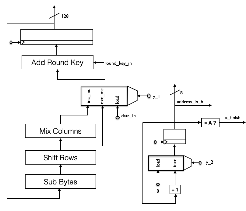
Following figure depicts the operational unit of the key expansion module including RAM module, counter and a component, from now on referred to as key expander, that is used for generation of the round keys.
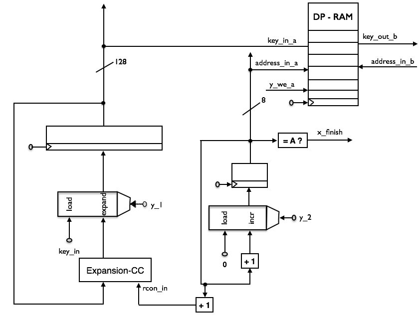
Key expansion module internals
The key expander includes a clocked 128-bit D flip-flop used to feed back the previous round key into a combinational circuit, labeled Expansion-CC. The Expansion-CC takes the previous round key and the counter value incremented by one which is used to internally generate a round constant. It then outputs the next round key that will be stored in the flip-flop after the next rising clock edge. Details of the round key generation can be taken from the official standard 3. The RAM module is used to store the sequentially generated 128-bit round keys at the address of the current counter value, incremented in each round. It is implemented as block RAM on the FPGA and has two several ports. One port is reading only and the other for writing the RAM module. Both reading and writing are synchronous.
A detailed description of the respective control unit is shown in following figure:
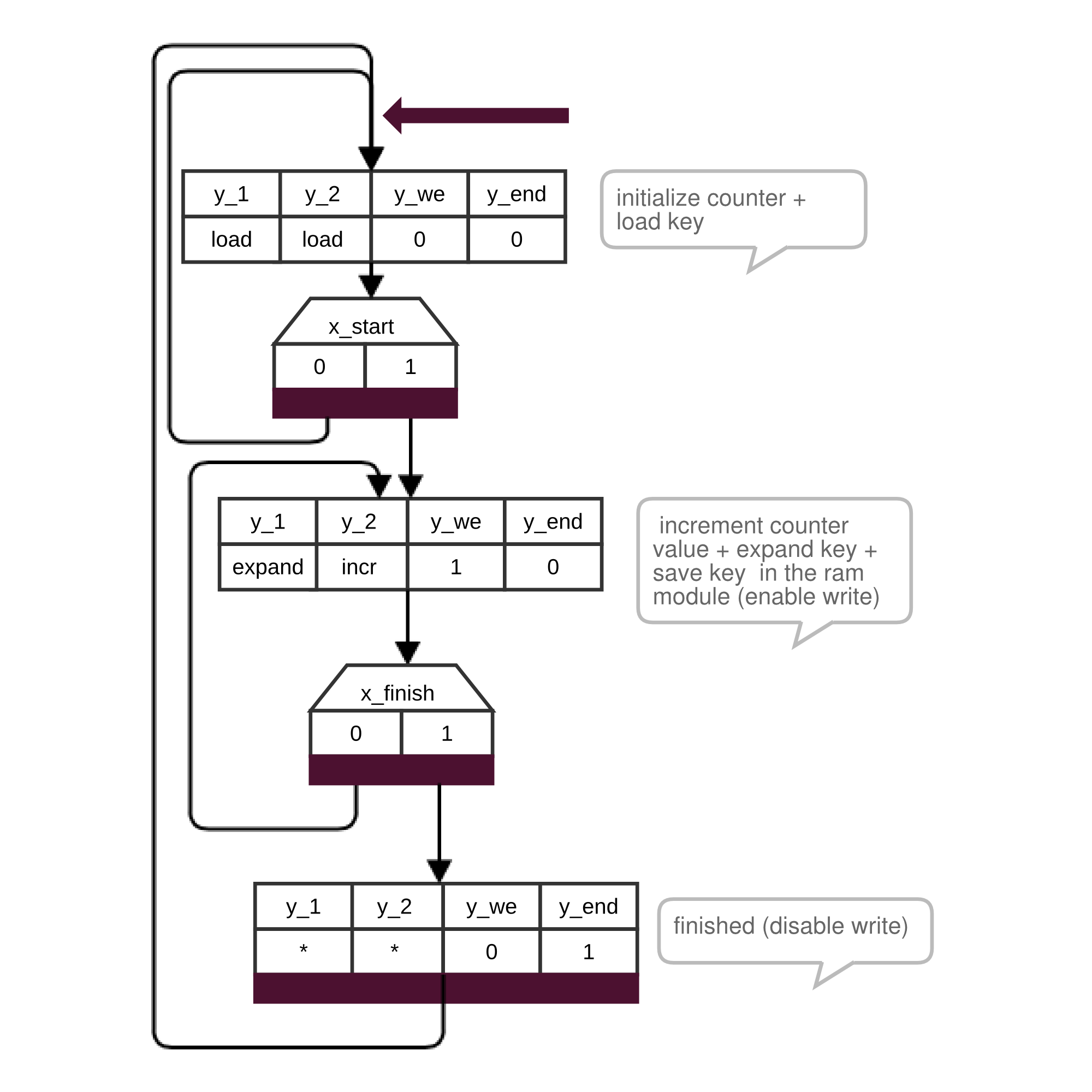
Key expansion module control unit states
In its initial state the control unit permanently loads the value from the d_in register into the register of the key expander. Furthermore it initializes the counter with zero. This is achieved by setting both multiplexers of the operational unit to load mode. If key expansion is invoked with the x_start flag the control unit jumps to the next state. Now, the counter value is incremented and the next round key is generated each clock cycle. Also write of RAM module is enabled to store the generated round keys. After all 11 round keys are stored in the RAM module the control unit disables write again and notifies the control unit of the AES core that key expansion is finished using the y_end signal.
Encryption Module
The operational unit of the encryption module is shown in the following figure. It consists of a counter and a component that includes the transformations of the AES Cipher. The transformations are applied multiple times to the 128-bit block that has to be encrypted.
Encryption module internals
The transformations are explained in detail in the official standard 3:
Sub Bytes - All bytes of the block are substituted. A single substitution can be implemented in hardware as a RAM module, serving as lookup table.
Shift Rows - Bytes are rearranged within some 32 bit words of the block. For implementation in hardware only rerouting of some signals is necessary.
Mix Columns - Transformation that operates on 32 bit words of the block. Can be implemented in hardware using several xor gates.
Add Round Key - The actual round key is XORed bitwise with the block. Can be implemented with one xor gate.
Following figure shows the behavior of the respective control unit control unit which is a Moore machine:
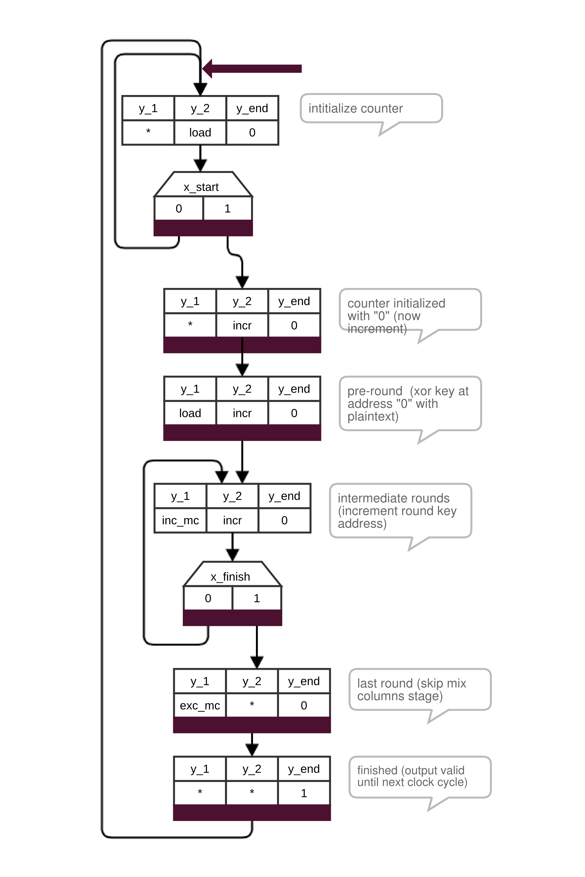
Encryption module control unit states
The control unit uses the operational unit to perform the AES Cipher algorithm, described in the official standard 3. At first the counter has to be initialized with zero. The output of the counter is connected to the read address port of the RAM, located in the key expansion module. After the counter is initialized with zero the control unit has to wait an additional clock cycle for the RAM to output the first round key, due to synchronous read. In the initial round the plaintext is loaded from the d_in register (see figure Encryption module internals) and XOR-ed with the first round key in the Add Round Key stage. The result is stored in the 128-bit register. Afterwards it is passed through the feed back loop 9 times including all transformation stages. The comparator connected to the counter notifies the control unit one clock cycle before the last round with the x_finish signal. In the last round the Mix Column stage is left out using the multiplexer. After the last round the control unit informs the higher-level control unit of the AES module that encryption is finished and that the output ciphertext_out is valid.
Decryption Module
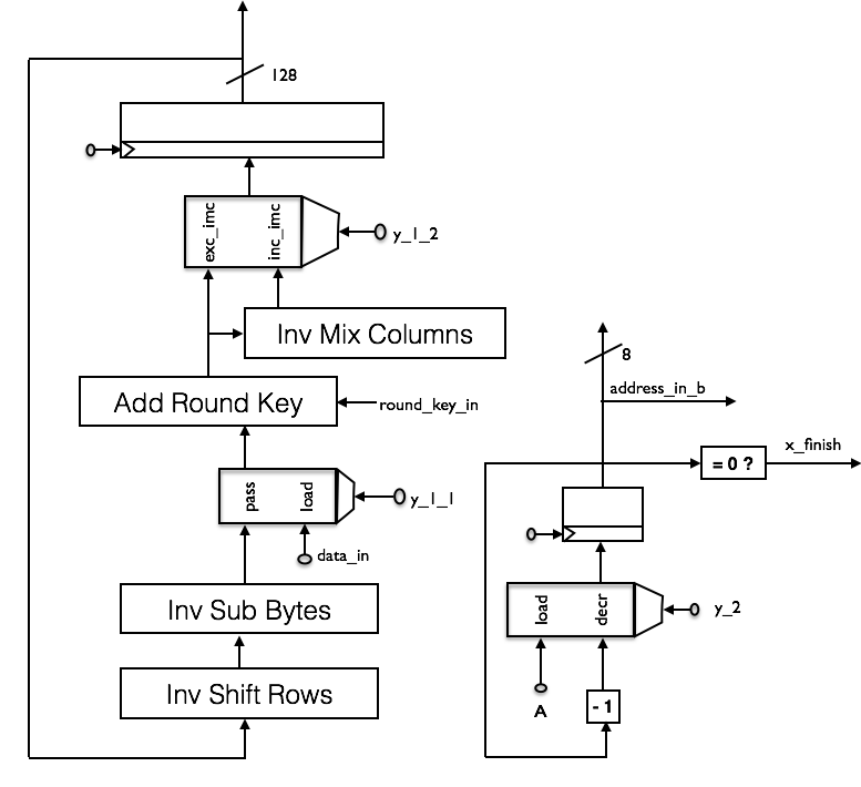
Following figure shows the operational unit of the decryption module.
Decryption module internals
The counter decrements the round key addresses in order to get the round keys in the reverse order. All transformations except from Add Round Key, which is just its own inverse, are now the inverse 3. Besides they are arranged in a different order.
The control unit, shown in figure below, performs the AES Inverse Cipher algorithm:
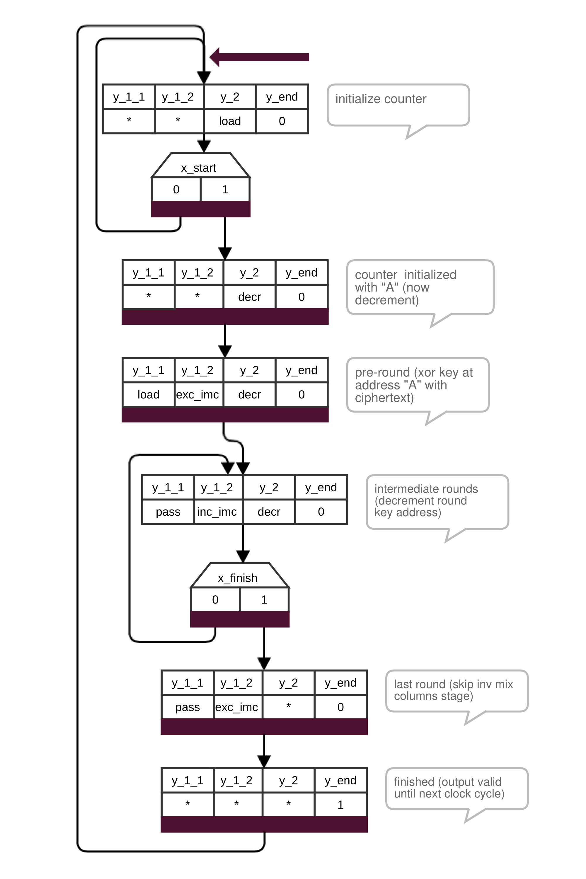
Decryption module control unit states
Aside from a few exceptions the control unit behaves similarly to the control unit of the encryption module. Details about the inverse operations, as well as the overall Inverse Cipher algorithm are explained in the official standard 3.
Results
Key expansion encryption, as well as decryption implemented in the AES core are operating directly on 128-bit blocks. Instead of operating on the full bit width, pipelining can be introduced to decrease the bit widths. Disadvantages of the non-pipelined approach, we used for our core, is a higher consumption of LUTs on the FPGA. According to the synthesis report of the Xilinx Vivado Design Suite 4, our core consumes totally 55% of the LUTs (9767 LUTs) on the FPGA of the ZYBO device we used for the AES acceleration:
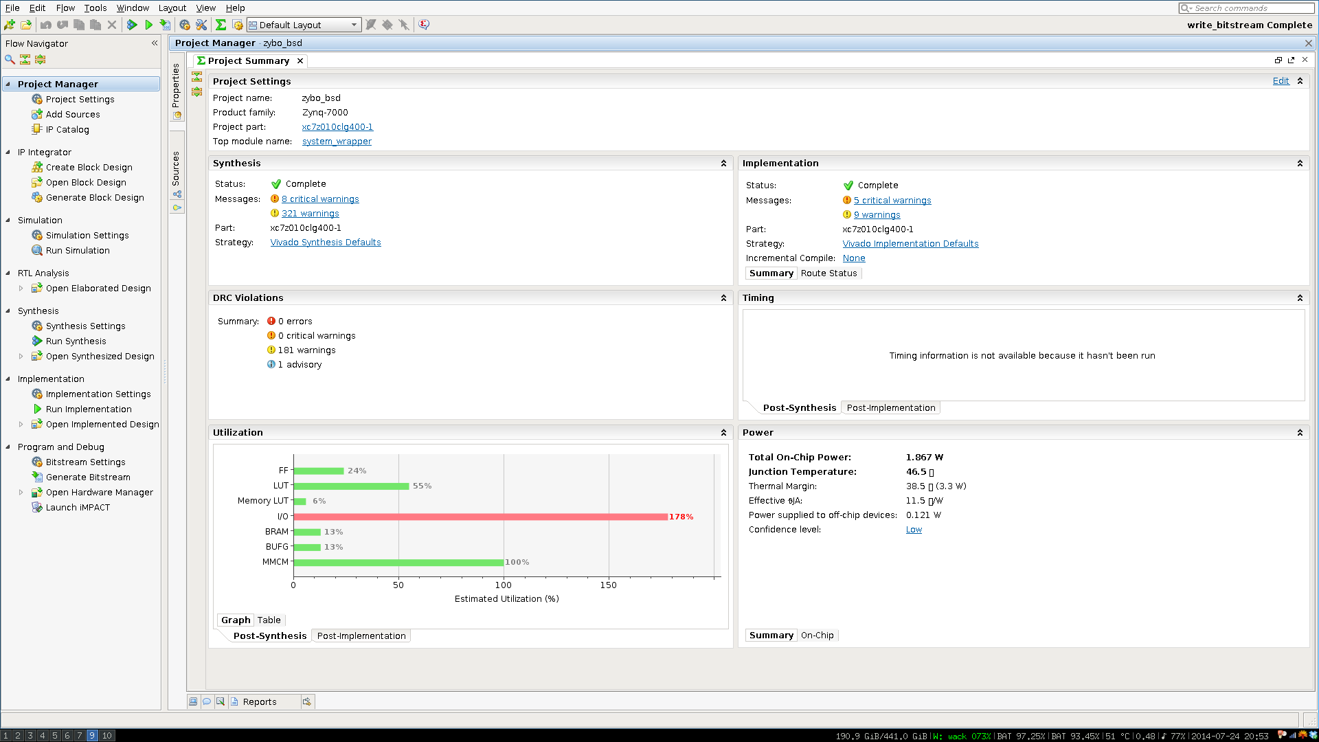
Resource utilization of AES core on ZYBO
However, we focused more on a performant approach with as less as possible clock cycles instead of saving space on the FGA. Encryption, decryption, as well as key expansion can be completed in 14 clock cycles. According to the timing analysis report of the Xilinx ISE Project Navigator 5, the core can be clocked with a frequency up to 276 MHz.
The kernel module is just a glue code between programmable logic and Linux kernel's Crypto API core. Whenever kernel performs context switch keys are set simply by writing the key to memory mapped regions of PL. Whenever a block needs to be encrypted or decrypted similar action is performed for the plaintext/ciphertext and the result is read back.
The block cipher operation mode is defined by the kernel module. Currently the simplest electronic codebook (ECB) and cipher-block chaining (CBC) are available. Moving CBC specific code to programmable logic might improve performance aswell, altough it's simply a XOR operation.
The measured throughput of CBC was about 2.5 MB/s which is roughly five to six times slower than software based solution. We believe that the problem lies in the latency introduced by AXI bus of magnitude of hundreds of CPU cycles. Using DMA might improve performance but there was no time to investigate DMA capabilities of this particular SoC. The other issue is that Crypto API exposes data as scatterlists and using DMA engine to feed the data to programmable logic might be challenging to implement 6.
Summary
Between the beginning of April and 10th of August several tasks were carried out as part of the project: Lauri investigated using Crypto API from userspace 7, compiling kernel for ZYBO 8 and using memory mapped input/output 9. Felix investigated AES standard and implemented 128-bit AES core. Angelo wrote Crypto API kernel module. Git repository was set up at Github and all code is available there 10. Offloading AES operations to the hardware works, but major work is still required to achieve the initial goal of doubling AES throughput.
- 1
http://www.apm.com/products/data-center/x-gene-family/x-gene/
- 2
ZYBO Reference Manual. DIGILENT, Pullman, WA. February 14, 2014
- 3(1,2,3,4,5,6,7,8)
Announcing the ADVANCED ENCRYPTION STANDARD (AES). Federal Information Processing Standards Publication 197. National Institute of Standards and Technology (NIST). November 26, 2001.
- 4
- 5
- 6
- 7
- 8
- 9
- 10