Getting started with Zynq-7000 boards
1.1 Introduction
Studying FPGA development is rather expensive process and so far the cheapest way to get started in my opinion is to get equipped with Digilent ZYBO development board, OV7670 camera, Salea logic analyzer, a breadboard, light emitting diodes, segment displays and some 220 ohm resistors. If you get lucky you can push it down to 200€ budget.
ZYBO is a Zynq-7000 SoC based board from Digilent. This is a little HOWTO for getting started with ZYBO, but this should serve well anyone who wants to get on the track with Zynq-7000 based boards such as Zedboard, Microzed, ZC702 evaluation board etc.
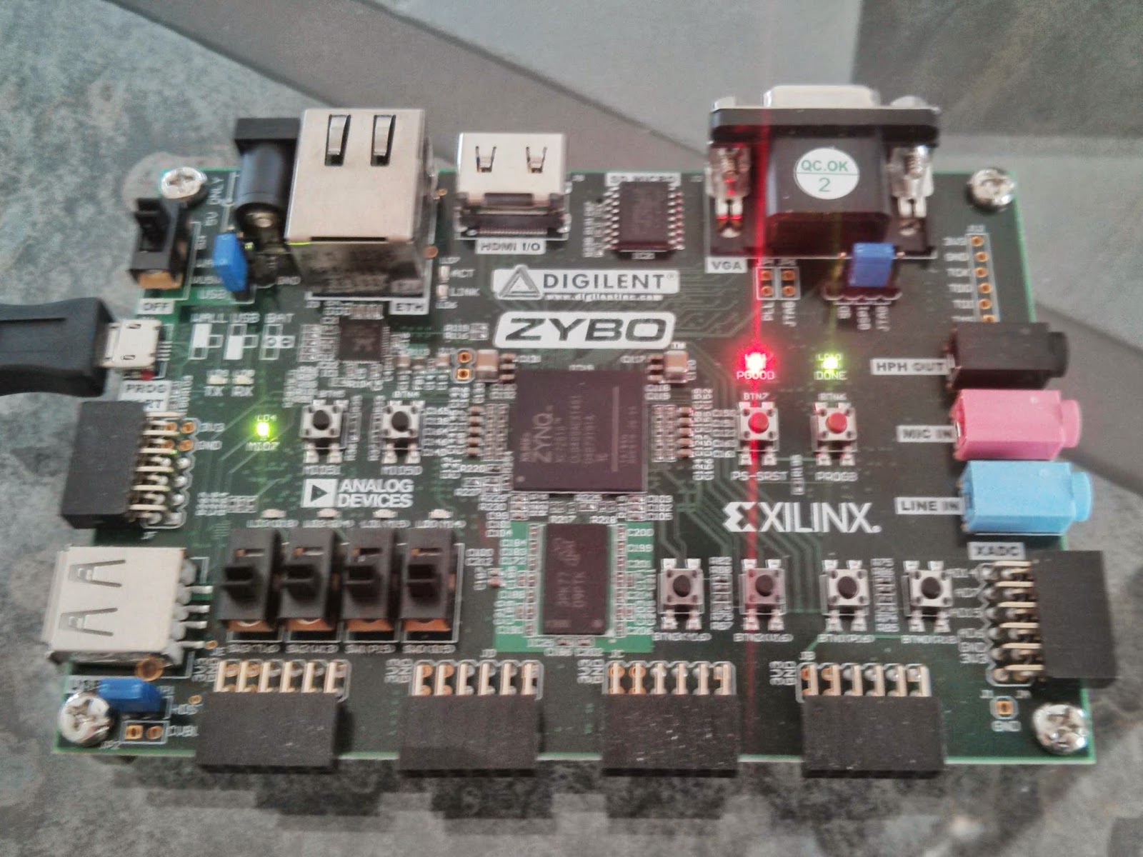
ZYBO is a Zynq-7000 SoC based entry level board.
Previously I attempted to outline detailed process of creating hardware design for ZYBO using Vivado, but as it turned out to consume significant amount of time spent on learning vendor specific stuff I decided to take the shortcut. Digilent provides ZYBO Base System Design 1 which includes prepared high level block design and IP cores for VGA output, HDMI output, and audio codec input/output.
As it is easier to remove useless blocks than to create block design from scratch this is recommended course of action. Base designs should be available for all Zynq-7000 boards from the corresponding hardware vendors. Otherwise you have to follow pretty complex guide to set up the high level block design from scratch 2.
1.2 Installing Vivado
Bitstream is a 2MB binary file which configures the programmable logic of ZYBO. Unfortunately the bitstream file can currently be compiled only with proprietary tools from Xilinx. When you're purchasing ZYBO from Digilent you have option to get 20 USD accessories kit for ZYBO which includes Vivado voucher. With the Voucher you get license for Vivado and it's updates for a year since the date of purchase. You can download Vivado at Xilinx web 3, just follow release notes to install Vivado and the license file Xilinx.lic. Note that license will be bound to the MAC address of the particular machine.
1.3 Working around Vivado quirks
If you encounter floating point formatting exception try disabling locales by appeding following to Vivado's settings64.sh:
export LANG=CIf you bump into NullPointerException while attempting to run Tools → Create Package and IP try to:
Open from main menu Tools → Project settings
Click on IP
Select Packager tab
Make sure Vendor field value if anything but (none)
1.4 Preparing bitstream
ZYBO Base System Design 1 includes all you need to compile the bitstream file for ZYBO. Uncompress the .zip file and open the project file source → vivado → hw → zybo_bsd → zybo_bsd.xpr with Vivado.
With newer Vivado versions you get notifications that IP blocks can be upgraded. Follow instructions on the screen to update the components. Once you have finished with the hardware design click on the lefthand panel Program and Debug → Generate Bitstream this will generate the 2MB blob that represents your FPGA configuration.
1.5 Preparing microSD card
The easiest is to use Xillinux as a starting point 4. Grab the Xillinux image and dump it to your microSD card. Note that previous contents of the card will be lost:
umount /dev/mmcblk0p*
wget -c http://xillybus.com/downloads/xillinux-1.3.img.gz
zcat xillinux-1.3.img.gz > /dev/mmcblk0
partprobe
Now you have your memory card populated with FAT32 filesystem for u-boot and ext4 filesystem which hosts Ubuntu 12.04 root filesystem. Next step is to place device tree definition file and first stage bootloader to the first (FAT32) filesystem:
wget -c http://xillybus.com/downloads/xillinux-eval-zybo-1.3v.zip
unzip xillinux-eval-zybo-1.3v.zip
mkdir /mnt/xillyboot
mount /dev/mmcblk0p1 /mnt/xillyboot
cp xillinux-eval-zybo-1.3v/bootfiles/boot.bin /mnt/xillyboot
cp xillinux-eval-zybo-1.3v/bootfiles/devicetree.dtb /mnt/xillyboot
cp path/to/zybo_base_system/source/vivado/hw/zybo_bsd/zybo_bsd.runs/impl_1/system_wrapper.bit /mnt/xillyboot/xillydemo.bit
umount /mnt/xillyboot
sync1.6 Booting Zynq-7000 board
In order to boot ZYBO the first (FAT32) filesystem has to contain:
boot.bin, the first stage bootloader shipper by Xillinux.
xillydemo.bit, the bitstream file produced by Vivado.
devicetree.dtb is the device tree which should be generated by Vivado but I currently can't seem to find a way to do it there. Instead I rely on the one provided by Xillinux.
uImage, the Linux kernel shipped by Xillinux.
Xillinux provided image has u-boot embedded to the the beginning of the card image which use the files mentioned above to set up hardware using the bitstream file, load kernel to RAM, load device tree to RAM and continue booting the kernel. Once kernel is up and running the kernel looks for root filesystem on the second partition which contains ext4 filesystem. If root filesystem is mounted successfully, the /sbin/init binary is invoked to continue the boot process.
If you have connected ZYBO via micro USB cable you can access the console via the built-in FTDI USB-UART bridge. Once you connect the cable to your Ubuntu laptop /dev/ttyUSB0 and /dev/ttyUSB1 should appear. Use picocom to connect to the virtual serial port:
sudo apt-get install picocom
sudo picocom -b 115200 /dev/ttyUSB0
1.7 Connecting via OpenSSH
As ZYBO has ethernet port onboard it makes sense to connect to the command-line via OpenSSH instead. Hook up an ethernet cable to ZYBO and connect it to a router or anything that provides DHCP service for automatically configuring the IP address of ZYBO. Otherwise you have to resort to manually configuring IP-s on your laptop, ZYBO and setting up masquerading and packet forwarding 5
Once the network is up and running you may install OpenSSH on ZYBO:
sudo apt-get install openssh-serverGenerate SSH keys using ssh-keygen on your laptop if you haven't done so yet and copy-paste the public key to ZYBO's /root/.ssh/authorized_keys2, this way you can avoid typing password every time you log in via OpenSSH 6.
As inserting and ejecting microSD card becomes eventually tedious I recommend using OpenSSH to transfer bitstream to the device. Make sure the first FAT32 partition is mounted at /boot on the Zynq-7000 board. OpenSSH should be installed on Ubuntu laptop by default, so you can simply issue:
scp \
  path/to/zybo_base_system/source/vivado/hw/zybo_bsd/zybo_bsd.runs/impl_1/system_wrapper.bit \
  root@xillinux:/boot/xillydemo.bit
This method of course does not work if the board does not boot at all and in that case you have to resort to inserting the microSD card to your laptop.
1.8 About device tree
Device tree concept was introduced in Linux 3.15 with the purpose of easing Linux adoption on embedded devices. In a traditional PC sophisticated mechanisms such as PCI and PCI Express are used to detect what kind of hardware has been connected and what drivers should be loaded for them. That is not the case for ARM as it does not have such peripherial arbitration capabilities. For usual ARM devices a device tree is provided from the vendor and it's available in the mainline Linux source tree. The programmable logic of Zynq-7000 SoC makes the hardware configurable to a high degree via the bitstream file and this is where the device tree is used to describe:
What kind of peripherial devices are connected via PL
Which memory addresses have been allocated to peripherial devices for memory mapped input/output
Which interrupts kernel knows about
Note that device tree is not necessary to enable memory mapped input/output. The Xillinux device tree seems to pass through the shared interrupt numbered 91. There are basically 16 peripherial devices that can be connected to that shared interrupt. Note that kernel module has to be written for handling hardware interrupts as it is not possible to hook up an interrupt handler from a userspace program. The kernel module may however translate interrupts to whatever a userspace program can understand eg. signals or blocking FIFO. Shared interrupt means that you need to use bitmasks to determine which event actually happened and afterwards still read the particular PL output from the memory mapped region.
1.9 Blinking LED-s!
Linux provides access to the physical memory addresses via /dev/mem. It's a character device whose lower 512MB represent the physical DDR RAM present on the board. Peripherial devices are accessible via memory ranges predefined in the bitstream using memory mapped input/output. The ZYBO base system Vivado project contains following setup:
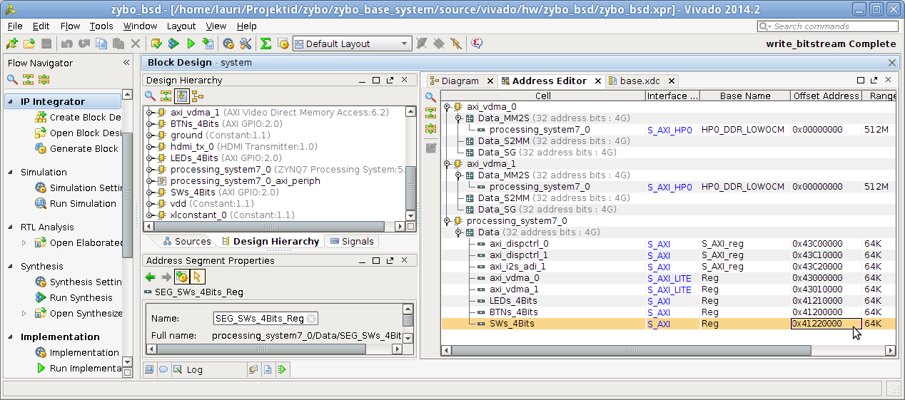
Address editor
To blink the LED-s on the board you can just grab the LEDs_4bits Offset Address from the Address Editor and using mmap() you can write and read that memory range as if it was regular array using following Python snippet.
from time import sleep
import mmap

with open("/dev/mem", "r+b") as f:
    mm = mmap.mmap(f.fileno(), 4, offset=0x41210000)
    while True:
        try:
            mm[0] = chr(0xff)
            sleep(0.2)
            mm[0] = chr(0x00)
            sleep(0.2)
        except KeyboardInterrupt:
            break
    mm.close()
Just dump the contents to a file and invoke with python at command-line.
In the source tree you'll find base.xdc which contains pin mapping for button block, switch block, LED block onboard and other preconfigured ports:
# Button block
set_property PACKAGE_PIN R18 [get_ports {btns_4bits_tri_i[0]}]
set_property PACKAGE_PIN P16 [get_ports {btns_4bits_tri_i[1]}]
set_property PACKAGE_PIN V16 [get_ports {btns_4bits_tri_i[2]}]
set_property PACKAGE_PIN Y16 [get_ports {btns_4bits_tri_i[3]}]
set_property IOSTANDARD LVCMOS33 [get_ports {btns_4bits_tri_i[*]}]

# LED block
set_property PACKAGE_PIN M14 [get_ports {leds_4bits_tri_o[0]}]
set_property PACKAGE_PIN M15 [get_ports {leds_4bits_tri_o[1]}]
set_property PACKAGE_PIN G14 [get_ports {leds_4bits_tri_o[2]}]
set_property PACKAGE_PIN D18 [get_ports {leds_4bits_tri_o[3]}]
set_property IOSTANDARD LVCMOS33 [get_ports {leds_4bits_tri_o[*]}]

# Switch block
set_property PACKAGE_PIN G15 [get_ports {sws_4bits_tri_i[0]}]
set_property PACKAGE_PIN P15 [get_ports {sws_4bits_tri_i[1]}]
set_property PACKAGE_PIN W13 [get_ports {sws_4bits_tri_i[2]}]
set_property PACKAGE_PIN T16 [get_ports {sws_4bits_tri_i[3]}]
set_property IOSTANDARD LVCMOS33 [get_ports {sws_4bits_tri_i[*]}]
Pmod connectors on the board are not by default connected to any ports. In addition to attaching port in the high level block design constraints have to be added for the corresponding pins. On the wide side ZYBO has standard Pmod connector JE connected via built-in 200Ω resistors and three hi-speed Pmod connectors JD, JC, JB with no resistors 7:
Two leftmost Pmod connectors JE, JD on the wider edge of ZYBO
Two rightmost Pmod connectors JC, JB on the wider edge of ZYBO
Pin mappings for other ports can be found in ZYBO reference manual 7 and they're virtually impossible to locate simply by searching the Internet.
2 Signal analysis using Sigrok
2.1 Introduction
Sigrok is an open-source software suite of signal analysis tools compromised of signal capture, protocol decoders and graphical tools. Sigrok's hardware support is pretty extensive and it's growing 9.
2.2 Installing
To install Sigrok on Ubuntu 14.04, enable their PPA repository:
sudo add-apt-repository ppa:jorik-kippendief/sigrok
sudo apt-get install pulseview
2.3 PulseView
Sigrok has command-line utilities for signal capture, but for newbies there is PulseView tool:
PulseView can parse various protocols such as I²C, SPI, UART etc.
2.4 Salea logic analyzer clones
Salea logic analyzer is a Cypress FX2 chipset based logic analyzer which can record up to 8 channels at 24MHz ranging from 0V to 5V.
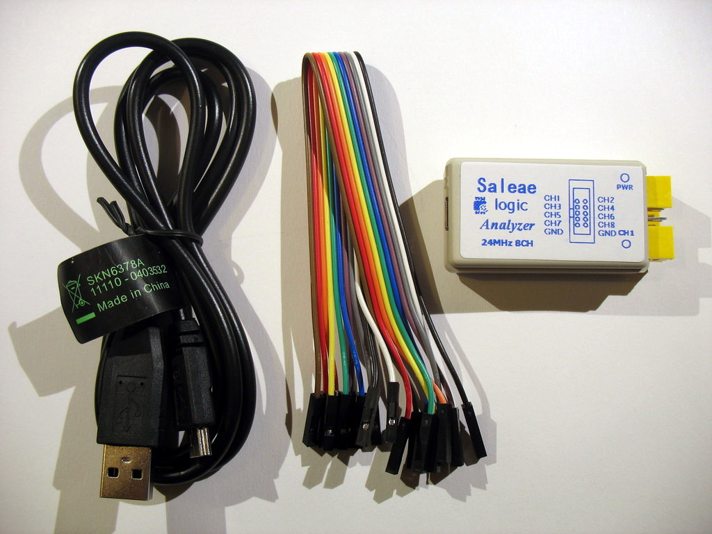
Salea logic analyzer can sample 8 channels at 24MHz.
It has been discontinued by Salea but its clones are still available, anything with that particular chipset works. In order to use that chipset with Sigrok tools firmware for the logic analyzer has to be installed, otherwise you get "Firmware upload failed" once you fire up PulseView:
sudo apt-get install sigrok-firmware-fx2lafwSalea logic analyzer clones can be purchased at eBay for less than 8€ per item 8.
2.5 Summary
Sigrok tools in conjunction with Salea logic analyzer clone can be used to interface FPGA design with already existing hardware and debug the design.
3 Decimal counter on ZYBO
3.1 Introduction
In this article I'll attempt to outline steps needed to convert VHDL design into a usable application on ZYBO board. I am going to assume that person attempting to follow the guide has familiarized herself with ZYBO basics and is using ZYBO Base System Design as starting point for the high level block design.
3.2 Sample files
In this case we're connecting two segment displays to Pmod connectors and use programmable fabric to convert bus frequency to seconds shown on the segment display:
library ieee;
use ieee.std_logic_1164.all;

entity frequency_divider is
    generic (
        RATIO : integer := 50000000);
    port (
        clk_in  : in  std_logic;
        reset   : in  std_logic;
        clk_out : out std_logic);
end;

architecture behavioral of frequency_divider is
    signal temporal: std_logic;
    signal counter : integer range 0 to RATIO := 0;
begin
    frequency_divider_process: process (reset, clk_in) begin
        if (reset = '1') then
            temporal <= '0';
            counter <= 0;
        elsif rising_edge(clk_in) then
            if (counter = RATIO) then
                temporal <= not(temporal);
                counter <= 0;
            else
                counter <= counter + 1;
            end if;
        end if;
    end process;
    clk_out <= temporal;
end;
BCD counter counts up to 10 and then overflows 11:
library ieee;
use ieee.std_logic_1164.all;
use ieee.numeric_std.all;

entity bcd_counter is
    port (
        clk_in  : in  std_logic;
        reset   : in  std_logic;
        inc     : in  std_logic;
        bcd     : out std_logic_vector(3 downto 0);
        clk_out : out std_logic);
end;

architecture behavioral of bcd_counter is
    signal temporal: std_logic;
    signal counter : integer range 0 to 10;
begin
    counter_process: process (reset, clk_in) begin
        if (reset = '1') then
            temporal <= '0';
            counter <= 0;
        elsif rising_edge(clk_in) then
            if inc = '1' then
                if (counter = 9) then
                    temporal <= '1';
                    counter <= 0;
                else
                    temporal <= '0';
                    counter <= counter + 1;
                end if;
            else
                if (counter = 0) then
                    temporal <= '1';
                    counter <= 9;
                else
                    temporal <= '0';
                    counter <= counter - 1;
                end if;
            end if;
        end if;
    end process;

    clk_out <= temporal;
    bcd <= std_logic_vector(to_unsigned(counter,4));
end;
Segment driver decodes BCD signal to segment display lanes:
library ieee;
use ieee.std_logic_1164.all;


entity bcd_segment_driver is
    port (
        bcd      : in  std_logic_vector(3 downto 0);
        segments : out std_logic_vector(6 downto 0));
end;

architecture behavioral of bcd_segment_driver is
begin
    segments <=
        "1111110" when bcd = "0000" else -- 0
        "0110000" when bcd = "0001" else -- 1
        "1101101" when bcd = "0010" else -- 2
        "1111001" when bcd = "0011" else -- 3
        "0110011" when bcd = "0100" else -- 4
        "1011011" when bcd = "0101" else -- 5
        "1011111" when bcd = "0110" else -- 6
        "1110000" when bcd = "0111" else -- 7
        "1111111" when bcd = "1000" else -- 8
        "1111011" when bcd = "1001" else -- 9
        "0000000";
end;
These files should be added by:
Open Tools → Create and Package IP
Select Package your current project
Point IP location to the folder containing these three files
Click Next
Click Finish
IP editor window should be opened now
Make adjustments to the VHDL code if necessary
Under Package IP tab open Review and Pacakage step, click Package IP button
3.3 Block design
In the Vivado high level block design window click Add IP, search for the IP core that was added and double click on it. Apply the same for remaining blocks. Use block design editor to combine frequency divider, BCD counter and BCD segment drivers:
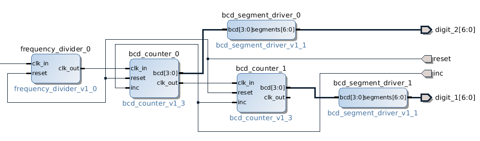
Frequency divider is connected to the ZYBO bus clocked at 50MHz
3.4 Pin mapping
Each ZYBO Pmod connector is basically connected to 8-bit port of programmable fabric. Each port's 1st pin is marked with square and pins 1-4 are in the top row and pins 5-8 are in the row closer to the PCB. Remaining four pins are connected to 3.3V and ground rails and they're explicitly marked on the board.
Pin mapping is described in ZYBO reference manual PDF documentation 10. Edit Constraints → constrs_1 → base.xdc to reflect your setup:
# Connect BTN0 to reset line
set_property PACKAGE_PIN R18 [get_ports {reset}]
set_property IOSTANDARD LVCMOS33 [get_ports {reset}]

# Pmod connector JB
set_property PACKAGE_PIN T20 [get_ports {digit_2[0]}]
set_property PACKAGE_PIN U20 [get_ports {digit_2[1]}]
set_property PACKAGE_PIN V20 [get_ports {digit_2[2]}]
set_property PACKAGE_PIN W20 [get_ports {digit_2[3]}]
set_property PACKAGE_PIN Y18 [get_ports {digit_2[4]}]
set_property PACKAGE_PIN Y19 [get_ports {digit_2[5]}]
set_property PACKAGE_PIN W18 [get_ports {digit_2[6]}]
set_property IOSTANDARD LVCMOS33 [get_ports {digit_2[*]}]

# Pmod connector JC
set_property PACKAGE_PIN V15 [get_ports {digit_1[0]}]
set_property PACKAGE_PIN W15 [get_ports {digit_1[1]}]
set_property PACKAGE_PIN T11 [get_ports {digit_1[2]}]
set_property PACKAGE_PIN T10 [get_ports {digit_1[3]}]
set_property PACKAGE_PIN W14 [get_ports {digit_1[4]}]
set_property PACKAGE_PIN Y14 [get_ports {digit_1[5]}]
set_property PACKAGE_PIN T12 [get_ports {digit_1[6]}]
set_property IOSTANDARD LVCMOS33 [get_ports {digit_1[*]}]

# Connect SW0 to increment/decrement toggle
set_property PACKAGE_PIN G15 [get_ports {inc}]
set_property IOSTANDARD LVCMOS33 [get_ports {inc}]
3.5 Final steps
Press Generate Bitstream in the left-hand panel under Program and Debug, the file will be written to zybo_base_system/source/vivado/hw/zybo_bsd/zybo_bsd.runs/impl_1/system_wrapper.bit. Transfer the file to the first FAT32 partition of the microSD card and reset the device.
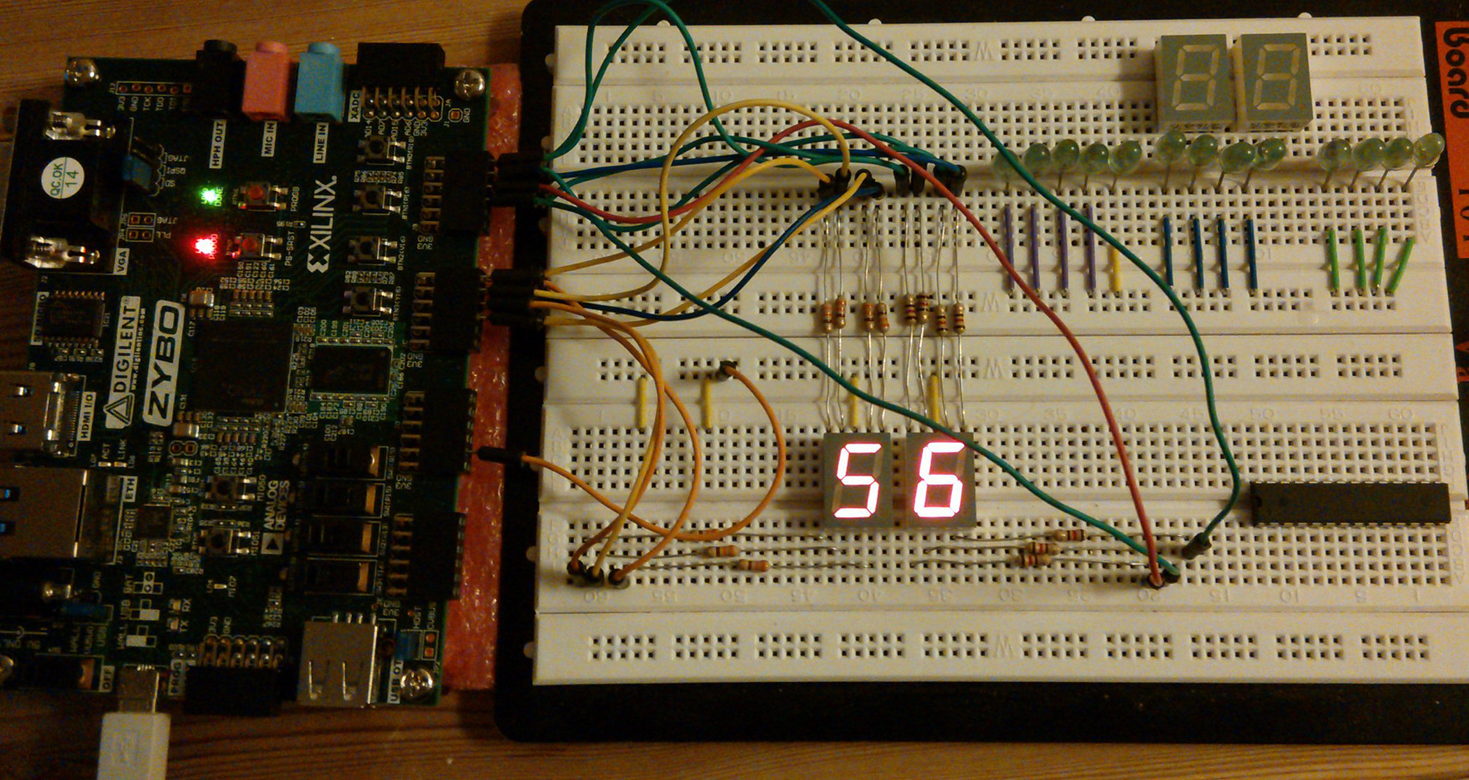
ZYBO in action
4 Piping OV7670 video to VGA output on ZYBO
4.1 Introduction
Before getting into more complex topics such as AXI Stream and direct memory access, it's recommended to first get familiar with pixel data encoding schemes and video timing signals. Hamsterworks has great examples for Zynq boards 12. In this example VGA frames are grabbed from OV7670 chipset based camera and stored in Block RAM based framebuffer.
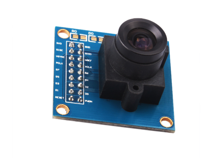
Omnivision OV7670 is a cheap 640x480 30fps camera module.
ZYBO is however more resource constrained so several modifications were required. In this case we're reducing the vertical resolution twofold since ZYBO does not have enough Block RAM to contain whole VGA frame. The example is basically working on ZYBO, but there are still few bugs that need to be ironed out.
4.2 Capture block
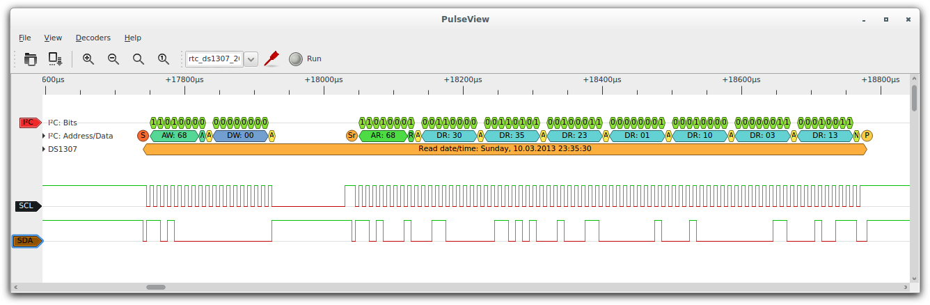
The capture block parses VSYNC and HREF signals and converts them into block RAM address. Pixel data is also a bit tricky - OV7670 transmits half of an 16-bit RGB (5:6:5) pixel during one PCLK cycle. Capture block latches the previous half and combines two halves into 12-bit RGB (4:4:4) pixel which is stored in block RAM. You are encouraged to use logic analyzer to debug video timing signals, as connecting wires to VGA output while display is connected is troublesome you might have to route extra pins onto Pmod connectors for debugging purposes.
----------------------------------------------------------------------------------
-- Engineer: Mike Field <hamster@snap.net.nz>
--
-- Description: Captures the pixels coming from the OV7670 camera and
--              Stores them in block RAM
----------------------------------------------------------------------------------
library ieee;
use ieee.std_logic_1164.ALL;
use ieee.NUMERIC_STD.ALL;

entity ov7670_capture is
    port (
        pclk  : in   std_logic;
        vsync : in   std_logic;
        href  : in   std_logic;
        d     : in   std_logic_vector ( 7 downto 0);
        addr  : out  std_logic_vector (17 downto 0);
        dout  : out  std_logic_vector (11 downto 0);
        we    : out  std_logic
    );
end ov7670_capture;

architecture behavioral of ov7670_capture is
   signal d_latch      : std_logic_vector(15 downto 0) := (others => '0');
   signal address      : std_logic_vector(18 downto 0) := (others => '0');
   signal address_next : std_logic_vector(18 downto 0) := (others => '0');
   signal wr_hold      : std_logic_vector( 1 downto 0)  := (others => '0');

begin
   addr <= address(18 downto 1);
   process(pclk)
   begin
      if rising_edge(pclk) then
         -- This is a bit tricky href starts a pixel transfer that takes 3 cycles
         --        Input   | state after clock tick
         --         href   | wr_hold    d_latch           d                 we address  address_next
         -- cycle -1  x    |    xx      xxxxxxxxxxxxxxxx  xxxxxxxxxxxxxxxx  x   xxxx     xxxx
         -- cycle 0   1    |    x1      xxxxxxxxRRRRRGGG  xxxxxxxxxxxxxxxx  x   xxxx     addr
         -- cycle 1   0    |    10      RRRRRGGGGGGBBBBB  xxxxxxxxRRRRRGGG  x   addr     addr
         -- cycle 2   x    |    0x      GGGBBBBBxxxxxxxx  RRRRRGGGGGGBBBBB  1   addr     addr+1

         if vsync = '1' then
            address <= (others => '0');
            address_next <= (others => '0');
            wr_hold <= (others => '0');
         else
            -- This should be a different order, but seems to be GRB!
            dout    <= d_latch(15 downto 12) & d_latch(10 downto 7) & d_latch(4 downto 1);
            address <= address_next;
            we      <= wr_hold(1);
            wr_hold <= wr_hold(0) & (href and not wr_hold(0));
            d_latch <= d_latch( 7 downto  0) & d;

            if wr_hold(1) = '1' then
               address_next <= std_logic_vector(unsigned(address_next)+1);
            end if;
         end if;
      end if;
   end process;
end behavioral;
4.3 Video output block
VGA output block generates HSYNC and VSYNC signals for the video outputs and corresponding input for the read address.
----------------------------------------------------------------------------------
-- Engineer: Mike Field <hamster@snap.net.nz>
--
-- Description: Generate analog 640x480 VGA, double-doublescanned from 19200 bytes of RAM
--
----------------------------------------------------------------------------------
library IEEE;
use IEEE.STD_LOGIC_1164.ALL;
use IEEE.NUMERIC_STD.ALL;

entity ov7670_vga is
    port (
        clk25       : in  STD_LOGIC;
        vga_red     : out STD_LOGIC_VECTOR(4 downto 0);
        vga_green   : out STD_LOGIC_VECTOR(5 downto 0);
        vga_blue    : out STD_LOGIC_VECTOR(4 downto 0);
        vga_hsync   : out STD_LOGIC;
        vga_vsync   : out STD_LOGIC;
        frame_addr  : out STD_LOGIC_VECTOR(17 downto 0);
        frame_pixel : in  STD_LOGIC_VECTOR(11 downto 0)
    );
end ov7670_vga;

architecture Behavioral of ov7670_vga is
   -- Timing constants
   constant hRez       : natural := 640;
   constant hStartSync : natural := 640+16;
   constant hEndSync   : natural := 640+16+96;
   constant hMaxCount  : natural := 800;

   constant vRez       : natural := 480;
   constant vStartSync : natural := 480+10;
   constant vEndSync   : natural := 480+10+2;
   constant vMaxCount  : natural := 480+10+2+33;

   constant hsync_active : std_logic := '0';
   constant vsync_active : std_logic := '0';

   signal hCounter : unsigned( 9 downto 0) := (others => '0');
   signal vCounter : unsigned( 9 downto 0) := (others => '0');
   signal address  : unsigned(18 downto 0) := (others => '0');
   signal blank    : std_logic := '1';

begin
   frame_addr <= std_logic_vector(address(18 downto 1));

   process(clk25)
   begin
      if rising_edge(clk25) then
         -- Count the lines and rows
         if hCounter = hMaxCount-1 then
            hCounter <= (others => '0');
            if vCounter = vMaxCount-1 then
               vCounter <= (others => '0');
            else
               vCounter <= vCounter+1;
            end if;
         else
            hCounter <= hCounter+1;
         end if;

         if blank = '0' then
            vga_red   <= frame_pixel(11 downto 8) & "0";
            vga_green <= frame_pixel( 7 downto 4) & "00";
            vga_blue  <= frame_pixel( 3 downto 0) & "0";
         else
            vga_red   <= (others => '0');
            vga_green <= (others => '0');
            vga_blue  <= (others => '0');
         end if;

         if vCounter  >= vRez then
            address <= (others => '0');
            blank <= '1';
         else
            if hCounter  < 640 then
               blank <= '0';
               address <= address+1;
            else
               blank <= '1';
            end if;
         end if;

         -- Are we in the hSync pulse? (one has been added to include frame_buffer_latency)
         if hCounter > hStartSync and hCounter <= hEndSync then
            vga_hSync <= hsync_active;
         else
            vga_hSync <= not hsync_active;
         end if;

         -- Are we in the vSync pulse?
         if vCounter >= vStartSync and vCounter < vEndSync then
            vga_vSync <= vsync_active;
         else
            vga_vSync <= not vsync_active;
         end if;
      end if;
   end process;
end Behavioral;
It essentially plays the role of video card in a PC.
4.4 Controller block
Omnivision OV7670 uses Omnivision Serial Camera Control Bus (SCCB) protocol to set up the camera parameters. SCCB actually is I²C-compliant interface, but avoids the usage of I²C brand due to licensing fees 13. The controller component is composed of three components: I²C bus master, OV7670 instructions and glue code.
The first one is used to emulate I²C bus master:
----------------------------------------------------------------------------------
-- Engineer: <mfield@concepts.co.nz
--
-- Description: Send the commands to the OV7670 over an I2C-like interface
----------------------------------------------------------------------------------

library ieee;
use ieee.std_logic_1164.all;
use ieee.numeric_std.all;

entity i2c_sender is
    port (
        clk   : in    std_logic;
        siod  : inout std_logic;
        sioc  : out   std_logic;
        taken : out   std_logic;
        send  : in    std_logic;
        id    : in    std_logic_vector(7 downto 0);
        reg   : in    std_logic_vector(7 downto 0);
        value : in    std_logic_vector(7 downto 0)
    );
end i2c_sender;

architecture behavioral of i2c_sender is
    -- this value gives a 254 cycle pause before the initial frame is sent
    signal   divider  : unsigned (7 downto 0) := "00000001";
    signal   busy_sr  : std_logic_vector(31 downto 0) := (others => '0');
    signal   data_sr  : std_logic_vector(31 downto 0) := (others => '1');
begin
    process(busy_sr, data_sr(31))
    begin
        if busy_sr(11 downto 10) = "10" or
           busy_sr(20 downto 19) = "10" or
           busy_sr(29 downto 28) = "10"  then
            siod <= 'Z';
        else
            siod <= data_sr(31);
        end if;
    end process;

    process(clk)
    begin
        if rising_edge(clk) then
            taken <= '0';
            if busy_sr(31) = '0' then
                SIOC <= '1';
                if send = '1' then
                    if divider = "00000000" then
                        data_sr <= "100" &   id & '0'  &   reg & '0' & value & '0' & "01";
                        busy_sr <= "111" & "111111111" & "111111111" & "111111111" & "11";
                        taken <= '1';
                    else
                        divider <= divider+1; -- this only happens on powerup
                    end if;
                end if;
            else

                case busy_sr(32-1 downto 32-3) & busy_sr(2 downto 0) is
                    when "111"&"111" => -- start seq #1
                        case divider(7 downto 6) is
                            when "00"   => SIOC <= '1';
                            when "01"   => SIOC <= '1';
                            when "10"   => SIOC <= '1';
                            when others => SIOC <= '1';
                        end case;
                    when "111"&"110" => -- start seq #2
                        case divider(7 downto 6) is
                            when "00"   => SIOC <= '1';
                            when "01"   => SIOC <= '1';
                            when "10"   => SIOC <= '1';
                            when others => SIOC <= '1';
                        end case;
                    when "111"&"100" => -- start seq #3
                        case divider(7 downto 6) is
                            when "00"   => SIOC <= '0';
                            when "01"   => SIOC <= '0';
                            when "10"   => SIOC <= '0';
                            when others => SIOC <= '0';
                        end case;
                    when "110"&"000" => -- end seq #1
                        case divider(7 downto 6) is
                            when "00"   => SIOC <= '0';
                            when "01"   => SIOC <= '1';
                            when "10"   => SIOC <= '1';
                            when others => SIOC <= '1';
                        end case;
                    when "100"&"000" => -- end seq #2
                        case divider(7 downto 6) is
                            when "00"   => SIOC <= '1';
                            when "01"   => SIOC <= '1';
                            when "10"   => SIOC <= '1';
                            when others => SIOC <= '1';
                        end case;
                    when "000"&"000" => -- Idle
                        case divider(7 downto 6) is
                            when "00"   => SIOC <= '1';
                            when "01"   => SIOC <= '1';
                            when "10"   => SIOC <= '1';
                            when others => SIOC <= '1';
                        end case;
                    when others      =>
                        case divider(7 downto 6) is
                            when "00"   => SIOC <= '0';
                            when "01"   => SIOC <= '1';
                            when "10"   => SIOC <= '1';
                            when others => SIOC <= '0';
                        end case;
                end case;

                if divider = "11111111" then
                    busy_sr <= busy_sr(32-2 downto 0) & '0';
                    data_sr <= data_sr(32-2 downto 0) & '1';
                    divider <= (others => '0');
                else
                    divider <= divider+1;
                end if;
            end if;
        end if;
    end process;
end behavioral;
The second one contains OV7670 setup instructions:
-- Company:
-- Engineer: Mike Field <hamster@sanp.net.nz>
--
-- Description: Register settings for the OV7670 Caamera (partially from OV7670.c
--              in the Linux Kernel
-- Edited by : Christopher Wilson <wilson@chrec.org>
------------------------------------------------------------------------------------
--
-- Notes:
-- 1) Regarding the WITH SELECT Statement:
--      WITH sreg(sel) SELECT
--           finished    <= '1' when x"FFFF",
--                        '0' when others;
-- This means the transfer is finished the first time sreg ends up as "FFFF",
-- I.E. Need Sequential Addresses in the below case statements
--
-- Common Debug Issues:
--
-- Red Appearing as Green / Green Appearing as Pink
-- Solution: Register Corrections Below
--
--
library IEEE;
use IEEE.STD_LOGIC_1164.ALL;
use IEEE.NUMERIC_STD.ALL;

entity ov7670_registers is
    Port ( clk      : in  STD_LOGIC;
           resend   : in  STD_LOGIC;
           advance  : in  STD_LOGIC;
           command  : out  std_logic_vector(15 downto 0);
           finished : out  STD_LOGIC);
end ov7670_registers;

architecture Behavioral of ov7670_registers is
   signal sreg   : std_logic_vector(15 downto 0);
   signal address : std_logic_vector(7 downto 0) := (others => '0');
begin
   command <= sreg;
   with sreg select finished  <= '1' when x"FFFF", '0' when others;

   process(clk)
   begin
      if rising_edge(clk) then
         if resend = '1' then
            address <= (others => '0');
         elsif advance = '1' then
            address <= std_logic_vector(unsigned(address)+1);
         end if;

         case address is
            when x"00" => sreg <= x"1280"; -- COM7   Reset
            when x"01" => sreg <= x"1280"; -- COM7   Reset
            when x"02" => sreg <= x"1204"; -- COM7   Size & RGB output
            when x"03" => sreg <= x"1100"; -- CLKRC  Prescaler - Fin/(1+1)
            when x"04" => sreg <= x"0C00"; -- COM3   Lots of stuff, enable scaling, all others off
            when x"05" => sreg <= x"3E00"; -- COM14  PCLK scaling off

            when x"06" => sreg <= x"8C00"; -- RGB444 Set RGB format
            when x"07" => sreg <= x"0400"; -- COM1   no CCIR601
             when x"08" => sreg <= x"4010"; -- COM15  Full 0-255 output, RGB 565
            when x"09" => sreg <= x"3a04"; -- TSLB   Set UV ordering,  do not auto-reset window
            when x"0A" => sreg <= x"1438"; -- COM9  - AGC Celling
            when x"0B" => sreg <= x"4f40"; --x"4fb3"; -- MTX1  - colour conversion matrix
            when x"0C" => sreg <= x"5034"; --x"50b3"; -- MTX2  - colour conversion matrix
            when x"0D" => sreg <= x"510C"; --x"5100"; -- MTX3  - colour conversion matrix
            when x"0E" => sreg <= x"5217"; --x"523d"; -- MTX4  - colour conversion matrix
            when x"0F" => sreg <= x"5329"; --x"53a7"; -- MTX5  - colour conversion matrix
            when x"10" => sreg <= x"5440"; --x"54e4"; -- MTX6  - colour conversion matrix
            when x"11" => sreg <= x"581e"; --x"589e"; -- MTXS  - Matrix sign and auto contrast
            when x"12" => sreg <= x"3dc0"; -- COM13 - Turn on GAMMA and UV Auto adjust
            when x"13" => sreg <= x"1100"; -- CLKRC  Prescaler - Fin/(1+1)
            when x"14" => sreg <= x"1711"; -- HSTART HREF start (high 8 bits)
            when x"15" => sreg <= x"1861"; -- HSTOP  HREF stop (high 8 bits)
            when x"16" => sreg <= x"32A4"; -- HREF   Edge offset and low 3 bits of HSTART and HSTOP
            when x"17" => sreg <= x"1903"; -- VSTART VSYNC start (high 8 bits)
            when x"18" => sreg <= x"1A7b"; -- VSTOP  VSYNC stop (high 8 bits)
            when x"19" => sreg <= x"030a"; -- VREF   VSYNC low two bits
            when x"1A" => sreg <= x"0e61"; -- COM5(0x0E) 0x61
            when x"1B" => sreg <= x"0f4b"; -- COM6(0x0F) 0x4B
            when x"1C" => sreg <= x"1602"; --
            when x"1D" => sreg <= x"1e37"; -- MVFP (0x1E) 0x07  -- FLIP AND MIRROR IMAGE 0x3x
            when x"1E" => sreg <= x"2102";
            when x"1F" => sreg <= x"2291";
            when x"20" => sreg <= x"2907";
            when x"21" => sreg <= x"330b";
            when x"22" => sreg <= x"350b";
            when x"23" => sreg <= x"371d";
            when x"24" => sreg <= x"3871";
            when x"25" => sreg <= x"392a";
            when x"26" => sreg <= x"3c78"; -- COM12 (0x3C) 0x78
            when x"27" => sreg <= x"4d40";
            when x"28" => sreg <= x"4e20";
            when x"29" => sreg <= x"6900"; -- GFIX (0x69) 0x00
            when x"2A" => sreg <= x"6b4a";
            when x"2B" => sreg <= x"7410";
            when x"2C" => sreg <= x"8d4f";
            when x"2D" => sreg <= x"8e00";
            when x"2E" => sreg <= x"8f00";
            when x"2F" => sreg <= x"9000";
            when x"30" => sreg <= x"9100";
            when x"31" => sreg <= x"9600";
            when x"32" => sreg <= x"9a00";
            when x"33" => sreg <= x"b084";
            when x"34" => sreg <= x"b10c";
            when x"35" => sreg <= x"b20e";
            when x"36" => sreg <= x"b382";
            when x"37" => sreg <= x"b80a";
            when others => sreg <= x"ffff";
         end case;
      end if;
   end process;
end Behavioral;
Third one contains glue code for the IP core that can actually be instantiated:
----------------------------------------------------------------------------------
-- Engineer: Mike Field <hamster@snap.net.nz>
--
-- Description: Controller for the OV760 camera - transferes registers to the
--              camera over an I2C like bus
----------------------------------------------------------------------------------
library IEEE;
use IEEE.STD_LOGIC_1164.ALL;
use IEEE.NUMERIC_STD.ALL;

entity ov7670_controller is
    Port ( clk   : in    STD_LOGIC;
                          resend :in    STD_LOGIC;
                          config_finished : out std_logic;
           sioc  : out   STD_LOGIC;
           siod  : inout STD_LOGIC;
           reset : out   STD_LOGIC;
           pwdn  : out   STD_LOGIC;
                          xclk  : out   STD_LOGIC
);
end ov7670_controller;

architecture Behavioral of ov7670_controller is
        COMPONENT ov7670_registers
        PORT(
                clk      : IN std_logic;
                advance  : IN std_logic;
                resend   : in STD_LOGIC;
                command  : OUT std_logic_vector(15 downto 0);
                finished : OUT std_logic
                );
        END COMPONENT;

        COMPONENT i2c_sender
        PORT(
                clk   : IN std_logic;
                send  : IN std_logic;
                taken : out std_logic;
                id    : IN std_logic_vector(7 downto 0);
                reg   : IN std_logic_vector(7 downto 0);
                value : IN std_logic_vector(7 downto 0);
                siod  : INOUT std_logic;
                sioc  : OUT std_logic
                );
        END COMPONENT;

        signal sys_clk  : std_logic := '0';
        signal command  : std_logic_vector(15 downto 0);
        signal finished : std_logic := '0';
        signal taken    : std_logic := '0';
        signal send     : std_logic;

        constant camera_address : std_logic_vector(7 downto 0) := x"42"; -- 42"; -- Device write ID - see top of page 11 of data sheet
begin
   config_finished <= finished;

        send <= not finished;
        Inst_i2c_sender: i2c_sender PORT MAP(
                clk   => clk,
                taken => taken,
                siod  => siod,
                sioc  => sioc,
                send  => send,
                id    => camera_address,
                reg   => command(15 downto 8),
                value => command(7 downto 0)
        );

        reset <= '1';                                           -- Normal mode
        pwdn  <= '0';                                           -- Power device up
        xclk  <= sys_clk;

        Inst_ov7670_registers: ov7670_registers PORT MAP(
                clk      => clk,
                advance  => taken,
                command  => command,
                finished => finished,
                resend   => resend
        );

        process(clk)
        begin
                if rising_edge(clk) then
                        sys_clk <= not sys_clk;
                end if;
        end process;
end Behavioral;4.5 Importing VHDL code
To insert VHDL code snippets into Vivado:
From the main menu select Tools → Create and Package IP, click Next.
Select Package a specified directory, click Next.
Locate the directory which contains VHDL files for IP location, click Next.
Set Project name to main component name.
Set Project location to the parent folder of the VHDL files.
Click Finish
Once you have added everything to the library it's time to instantiate the code in the design, for each component add the corresponding block:
Click on Open Block Design under IP Integrator to open up the high level block design.
Right click in the designer area and select Add IP...
Locate the components added earlier
Repeat same steps for all components
Next step is to insert block RAM, clocking wizard and connect the components.
4.6 Instantiating block RAM
Since block RAM is highly platform specific a Xilinx block has to be inserted. Right click in the high level design → Add IP... → Block Memory Generator to insert block RAM. Right click on the block → Customize block... opens up the dialog for editing block RAM parameters.
Stand Alone mode makes it possible to generate Simple Dual Port RAM which is essentially memory with write port and read port. Port width refers to amount of bits that can be read/written at once or in other words the size of a memory slot. Port depth refers to count of such slots which translates to address bit width.
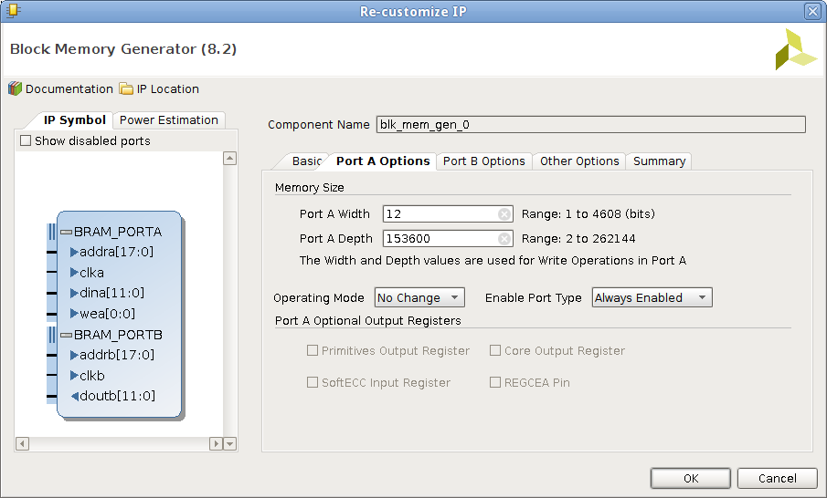
Block RAM generator parameters
4.7 Routing pins
The base.xdc important chunks are following:
# Debounce button and config finished LED
set_property PACKAGE_PIN R18 [get_ports button_debounce]
set_property PACKAGE_PIN M14 [get_ports led_config_finished]

# Top JE
set_property PACKAGE_PIN H15 [get_ports ov7670_reset]
set_property PACKAGE_PIN J16 [get_ports {ov7670_d[1]}]
set_property PACKAGE_PIN W16 [get_ports {ov7670_d[3]}]
set_property PACKAGE_PIN V12 [get_ports {ov7670_d[5]}]

# Bottom JE
set_property PACKAGE_PIN Y17 [get_ports ov7670_pwdn]
set_property PACKAGE_PIN T17 [get_ports {ov7670_d[0]}]
set_property PACKAGE_PIN U17 [get_ports {ov7670_d[2]}]
set_property PACKAGE_PIN V13 [get_ports {ov7670_d[4]}]

# Top JD
set_property PACKAGE_PIN R14 [get_ports {ov7670_d[7]}]
set_property PACKAGE_PIN P14 [get_ports ov7670_pclk]
set_property PACKAGE_PIN T15 [get_ports ov7670_vsync]
set_property PACKAGE_PIN T14 [get_ports ov7670_sioc]

# Bottom JD
set_property PACKAGE_PIN V18 [get_ports {ov7670_d[6]}]
set_property PACKAGE_PIN V17 [get_ports ov7670_xclk]
set_property PACKAGE_PIN U15 [get_ports ov7670_href]
set_property PACKAGE_PIN U14 [get_ports ov7670_siod]

# Red channel of VGA output
set_property PACKAGE_PIN M19 [get_ports {RED_O[0]}]
set_property PACKAGE_PIN L20 [get_ports {RED_O[1]}]
set_property PACKAGE_PIN J20 [get_ports {RED_O[2]}]
set_property PACKAGE_PIN G20 [get_ports {RED_O[3]}]
set_property PACKAGE_PIN F19 [get_ports {RED_O[4]}]

# Green channel of VGA output
set_property PACKAGE_PIN H18 [get_ports {GREEN_O[0]}]
set_property PACKAGE_PIN N20 [get_ports {GREEN_O[1]}]
set_property PACKAGE_PIN L19 [get_ports {GREEN_O[2]}]
set_property PACKAGE_PIN J19 [get_ports {GREEN_O[3]}]
set_property PACKAGE_PIN H20 [get_ports {GREEN_O[4]}]
set_property PACKAGE_PIN F20 [get_ports {GREEN_O[5]}]
# Blue channel of VGA output
set_property PACKAGE_PIN P20 [get_ports {BLUE_O[0]}]
set_property PACKAGE_PIN M20 [get_ports {BLUE_O[1]}]
set_property PACKAGE_PIN K19 [get_ports {BLUE_O[2]}]
set_property PACKAGE_PIN J18 [get_ports {BLUE_O[3]}]
set_property PACKAGE_PIN G19 [get_ports {BLUE_O[4]}]

# Horizontal and vertical synchronization of VGA output
set_property PACKAGE_PIN P19 [get_ports HSYNC_O]
set_property PACKAGE_PIN R19 [get_ports VSYNC_O]

# Voltage levels
set_property IOSTANDARD LVCMOS33 [get_ports button_debounce]
set_property IOSTANDARD LVCMOS33 [get_ports led_config_finished]
set_property IOSTANDARD LVCMOS33 [get_ports ov7670_pclk]
set_property IOSTANDARD LVCMOS33 [get_ports ov7670_sioc]
set_property IOSTANDARD LVCMOS33 [get_ports ov7670_vsync]
set_property IOSTANDARD LVCMOS33 [get_ports ov7670_reset]
set_property IOSTANDARD LVCMOS33 [get_ports ov7670_pwdn]
set_property IOSTANDARD LVCMOS33 [get_ports ov7670_href]
set_property IOSTANDARD LVCMOS33 [get_ports ov7670_xclk]
set_property IOSTANDARD LVCMOS33 [get_ports ov7670_siod]
set_property IOSTANDARD LVCMOS33 [get_ports {ov7670_d[*]}]
set_property IOSTANDARD LVCMOS33 [get_ports {RED_O[*]}]
set_property IOSTANDARD LVCMOS33 [get_ports {GREEN_O[*]}]
set_property IOSTANDARD LVCMOS33 [get_ports {BLUE_O[*]}]
set_property IOSTANDARD LVCMOS33 [get_ports HSYNC_O]
set_property IOSTANDARD LVCMOS33 [get_ports VSYNC_O]

# Magic
set_property CLOCK_DEDICATED_ROUTE FALSE [get_nets ov7670_pclk_IBUF]
Using the pin mapping above the camera can be connected cleanly to the board:
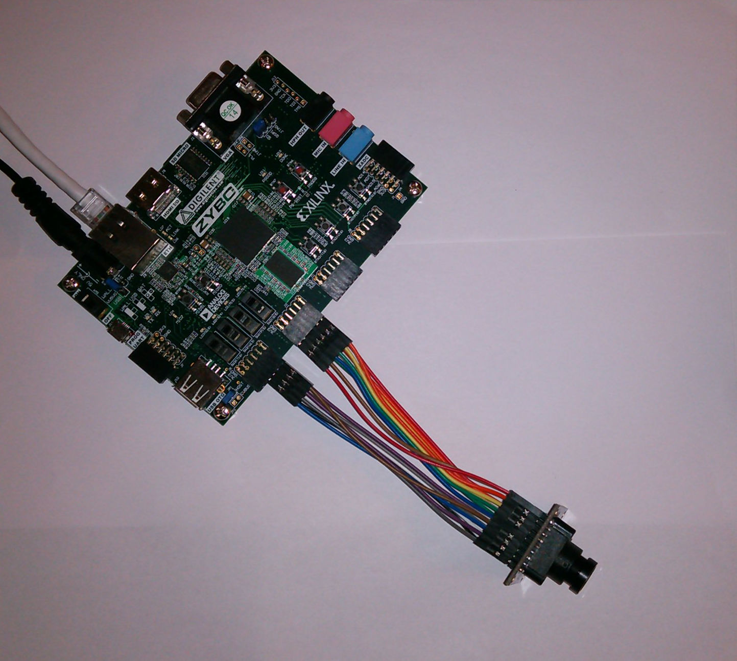
Omnivision OV7670 attached to Pmod connectors JD and JE.
Remember to connect GND and 3.3V rails of the ZYBO to cameras GND and 3.3V rails.
4.8 Final high level design
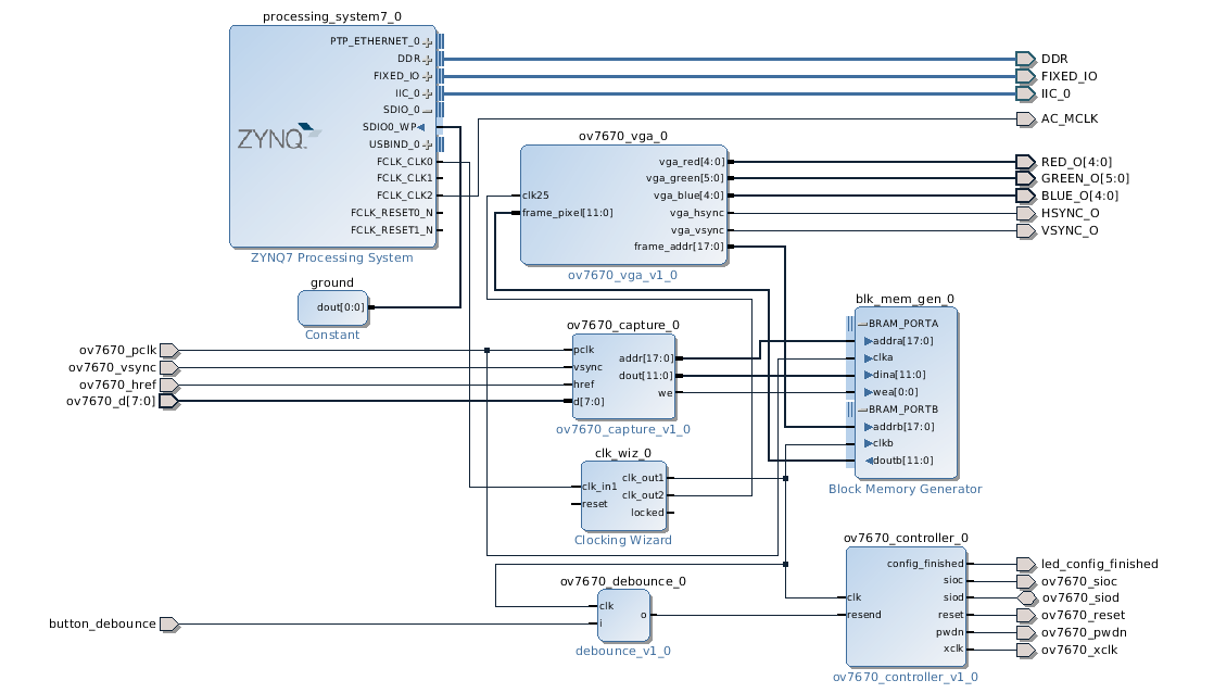
High level design
Click on Generate bitstream button and transfer resulting bitstream file to the boot partition and restart ZYBO.
4.9 Summary
If you've connected camera correctly you should see the video feed from the camera on the screen attached to VGA output. Capture and controller blocks can be re-used in other examples involving Omnivision OV7670 camera, so it's important to get expected outcome at this point.
5 AXI Direct Memory Access
5.1 Introduction
Getting started with direct memory access on Xilinx boards may be initially overwhelming. First of all Xilinx distinguishes AXI DMA and AXI VDMA in programmable fabric. AXI DMA refers to traditional FPGA direct memory access which roughly corresponds to transferring arbitrary streams of bytes from FPGA to a slice of DDR memory and vice versa. VDMA refers to video DMA which adds mechanisms to handle frame synchronization using ring buffer in DDR, on-the-fly video resolution changes, cropping and zooming. Video DMA is covered in next article. In addition to AXI DMA and AXI VDMA there is a DMA engine built into the ARM core which is also out of the scope of this article. Both AXI DMA and AXI VDMA have optional scatter-gather support which means that instead of writing memory addresses or framebuffer addresses to control registers the DMA controller grabs them from linked list in DDR memory. Scatter-gather features are out of scope of this article.
5.2 Internals
AXI DMA distinguishes two channels: MM2S (memory-mapped to stream) transports data from DDR memory to FPGA and S2MM (stream to memory-mapped) transports arbitrary data stream to DDR memory.
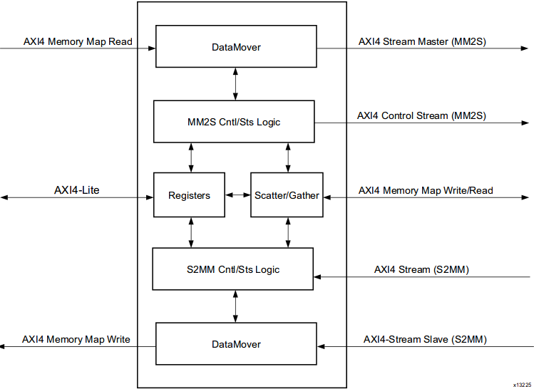
AXI DMA internals
5.3 Minimal working hardware
The simplest way to instantiate AXI DMA on Zynq-7000 based boards is to take board vendor's base design, strip unnecessary components, add AXI Direct Memory Access IP-core and connect the output stream port to it's input stream port. This essentially implements memcpy functionality which can be triggered from ARM core but offloaded to programmable fabric.
AXI Direct Memory Access stream output is looped back to stream input
To be more precise, following is the corresponding high level block design. High speed clock line is highlighted in yellow as it runs on higher frequency of 150MHz while the general purpose port runs at 100MHz. Clock domain errors can usually be tracked back to conflicting clock lines. This is further explained in the end of this article.
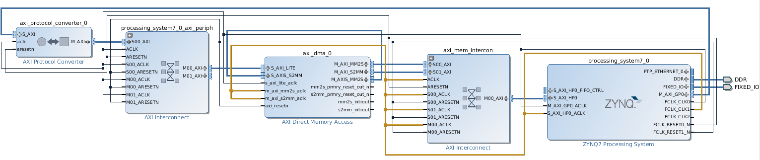
High level block design corresponding to abstract design presented earlier
In the AXI Direct Memory Access IP-core customization dialog read channel and write channel correspond respectively to MM2S and S2MM portions of the DMA block. Memory map data width of 32 bits means that 4 bytes will be transferred during one bus cycle. This means the tdata port of the stream interface will be 32 bits wide.
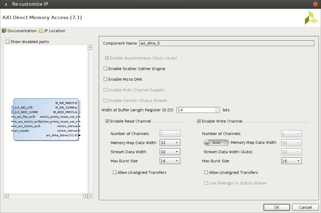
Both read/write channels are enabled and scatter-gather engine is disabled
AXI Direct Memory Access component's control register, status register and transfer address registers are accessible via the AXI Lite slave port which is memory mapped to address range of 0x40400000 - 0x4040FFFF. The whole memory range of 0x00000000-0x1FFFFFFF is accessible via both stream to memory-mapped and memory-mapped to stream channel. AXI DMA 14 documentation has the offsets of the registers accessible via AXI Lite port. In this case MM2S control register of 32-bits is accessible at 0x40400000, MM2S status register of 32-bits at 0x40400004 and so forth.

Important
Note that customizing the AXI Direct Memory Access IP-core parameters causes memory ranges to be reset under Address Editor!
5.4 Minimal working software
When it comes to writing C code I see alarming tendency of defaulting to vendor provided components: stand-alone binary compilers, Linux distributions, board support packages, wrappers while avoiding learning what actually happens in the hardware/software.
As described in my earlier article physical memory can be accessed in Linux via /dev/mem block device. This makes it possible to access AXI Lite registers simply by reading/writing to a memory mapped range from /dev/mem. To use DMA component minimally four steps have to be taken:
Start the DMA channel (MM2S, S2MM or both) by writing 1 to control register
Write start/destination addresses to corresponding registers
To initiate the transfer(s) write transfer length(s) to corresponding register(s).
Monitor status register for IOC_Irq flag.
In this case we're copying 32 bytes from physical address of 0x0E000000 to physical addres of 0x0F000000. Note that kernel may allocate memory for other processes in that range and that is the primary reason to write a kernel module which would request_mem_region so no other processes would overlap with the memory range. Besides reserving memory ranges the kernel module provides a sanitized way of accessing the hardware from userspace applications via /dev/blah block devices.
/**
 * Proof of concept offloaded memcopy using AXI Direct Memory Access v7.1
 */

#include <stdio.h>
#include <unistd.h>
#include <fcntl.h>
#include <termios.h>
#include <sys/mman.h>

#define MM2S_CONTROL_REGISTER 0x00
#define MM2S_STATUS_REGISTER 0x04
#define MM2S_START_ADDRESS 0x18
#define MM2S_LENGTH 0x28

#define S2MM_CONTROL_REGISTER 0x30
#define S2MM_STATUS_REGISTER 0x34
#define S2MM_DESTINATION_ADDRESS 0x48
#define S2MM_LENGTH 0x58

unsigned int dma_set(unsigned int* dma_virtual_address, int offset, unsigned int value) {
    dma_virtual_address[offset>>2] = value;
}

unsigned int dma_get(unsigned int* dma_virtual_address, int offset) {
    return dma_virtual_address[offset>>2];
}

int dma_mm2s_sync(unsigned int* dma_virtual_address) {
    unsigned int mm2s_status =  dma_get(dma_virtual_address, MM2S_STATUS_REGISTER);
    while(!(mm2s_status & 1<<12) || !(mm2s_status & 1<<1) ){
        dma_s2mm_status(dma_virtual_address);
        dma_mm2s_status(dma_virtual_address);

        mm2s_status =  dma_get(dma_virtual_address, MM2S_STATUS_REGISTER);
    }
}

int dma_s2mm_sync(unsigned int* dma_virtual_address) {
    unsigned int s2mm_status = dma_get(dma_virtual_address, S2MM_STATUS_REGISTER);
    while(!(s2mm_status & 1<<12) || !(s2mm_status & 1<<1)){
        dma_s2mm_status(dma_virtual_address);
        dma_mm2s_status(dma_virtual_address);

        s2mm_status = dma_get(dma_virtual_address, S2MM_STATUS_REGISTER);
    }
}

void dma_s2mm_status(unsigned int* dma_virtual_address) {
    unsigned int status = dma_get(dma_virtual_address, S2MM_STATUS_REGISTER);
    printf("Stream to memory-mapped status (0x%08x@0x%02x):", status, S2MM_STATUS_REGISTER);
    if (status & 0x00000001) printf(" halted"); else printf(" running");
    if (status & 0x00000002) printf(" idle");
    if (status & 0x00000008) printf(" SGIncld");
    if (status & 0x00000010) printf(" DMAIntErr");
    if (status & 0x00000020) printf(" DMASlvErr");
    if (status & 0x00000040) printf(" DMADecErr");
    if (status & 0x00000100) printf(" SGIntErr");
    if (status & 0x00000200) printf(" SGSlvErr");
    if (status & 0x00000400) printf(" SGDecErr");
    if (status & 0x00001000) printf(" IOC_Irq");
    if (status & 0x00002000) printf(" Dly_Irq");
    if (status & 0x00004000) printf(" Err_Irq");
    printf("\n");
}

void dma_mm2s_status(unsigned int* dma_virtual_address) {
    unsigned int status = dma_get(dma_virtual_address, MM2S_STATUS_REGISTER);
    printf("Memory-mapped to stream status (0x%08x@0x%02x):", status, MM2S_STATUS_REGISTER);
    if (status & 0x00000001) printf(" halted"); else printf(" running");
    if (status & 0x00000002) printf(" idle");
    if (status & 0x00000008) printf(" SGIncld");
    if (status & 0x00000010) printf(" DMAIntErr");
    if (status & 0x00000020) printf(" DMASlvErr");
    if (status & 0x00000040) printf(" DMADecErr");
    if (status & 0x00000100) printf(" SGIntErr");
    if (status & 0x00000200) printf(" SGSlvErr");
    if (status & 0x00000400) printf(" SGDecErr");
    if (status & 0x00001000) printf(" IOC_Irq");
    if (status & 0x00002000) printf(" Dly_Irq");
    if (status & 0x00004000) printf(" Err_Irq");
    printf("\n");
}

void memdump(void* virtual_address, int byte_count) {
    char *p = virtual_address;
    int offset;
    for (offset = 0; offset < byte_count; offset++) {
        printf("%02x", p[offset]);
        if (offset % 4 == 3) { printf(" "); }
    }
    printf("\n");
}


int main() {
    int dh = open("/dev/mem", O_RDWR | O_SYNC); // Open /dev/mem which represents the whole physical memory
    unsigned int* virtual_address = mmap(NULL, 65535, PROT_READ | PROT_WRITE, MAP_SHARED, dh, 0x40400000); // Memory map AXI Lite register block
    unsigned int* virtual_source_address  = mmap(NULL, 65535, PROT_READ | PROT_WRITE, MAP_SHARED, dh, 0x0e000000); // Memory map source address
    unsigned int* virtual_destination_address = mmap(NULL, 65535, PROT_READ | PROT_WRITE, MAP_SHARED, dh, 0x0f000000); // Memory map destination address

    virtual_source_address[0]= 0x11223344; // Write random stuff to source block
    memset(virtual_destination_address, 0, 32); // Clear destination block

    printf("Source memory block:      "); memdump(virtual_source_address, 32);
    printf("Destination memory block: "); memdump(virtual_destination_address, 32);

    printf("Resetting DMA\n");
    dma_set(virtual_address, S2MM_CONTROL_REGISTER, 4);
    dma_set(virtual_address, MM2S_CONTROL_REGISTER, 4);
    dma_s2mm_status(virtual_address);
    dma_mm2s_status(virtual_address);

    printf("Halting DMA\n");
    dma_set(virtual_address, S2MM_CONTROL_REGISTER, 0);
    dma_set(virtual_address, MM2S_CONTROL_REGISTER, 0);
    dma_s2mm_status(virtual_address);
    dma_mm2s_status(virtual_address);

    printf("Writing destination address\n");
    dma_set(virtual_address, S2MM_DESTINATION_ADDRESS, 0x0f000000); // Write destination address
    dma_s2mm_status(virtual_address);

    printf("Writing source address...\n");
    dma_set(virtual_address, MM2S_START_ADDRESS, 0x0e000000); // Write source address
    dma_mm2s_status(virtual_address);

    printf("Starting S2MM channel with all interrupts masked...\n");
    dma_set(virtual_address, S2MM_CONTROL_REGISTER, 0xf001);
    dma_s2mm_status(virtual_address);

    printf("Starting MM2S channel with all interrupts masked...\n");
    dma_set(virtual_address, MM2S_CONTROL_REGISTER, 0xf001);
    dma_mm2s_status(virtual_address);

    printf("Writing S2MM transfer length...\n");
    dma_set(virtual_address, S2MM_LENGTH, 32);
    dma_s2mm_status(virtual_address);

    printf("Writing MM2S transfer length...\n");
    dma_set(virtual_address, MM2S_LENGTH, 32);
    dma_mm2s_status(virtual_address);

    printf("Waiting for MM2S synchronization...\n");
    dma_mm2s_sync(virtual_address);

    printf("Waiting for S2MM sychronization...\n");
    dma_s2mm_sync(virtual_address); // If this locks up make sure all memory ranges are assigned under Address Editor!

    dma_s2mm_status(virtual_address);
    dma_mm2s_status(virtual_address);

    printf("Destination memory block: "); memdump(virtual_destination_address, 32);
}
Successful run should look something like this:
Source memory block:      44332211 7dcddfdf 5a7fefa4 36aa3c9b ca2eea6a 5bf64f81 ebf7ffbb b7f710d2
Destination memory block: 00000000 00000000 00000000 00000000 00000000 00000000 00000000 00000000
Resetting DMA
Stream to memory-mapped status (0x00000001@0x34): halted
Memory-mapped to stream status (0x00000001@0x04): halted
Halting DMA
Stream to memory-mapped status (0x00000001@0x34): halted
Memory-mapped to stream status (0x00000001@0x04): halted
Writing destination address
Stream to memory-mapped status (0x00000001@0x34): halted
Writing source address...
Memory-mapped to stream status (0x00000001@0x04): halted
Starting S2MM channel with all interrupts masked...
Stream to memory-mapped status (0x00000000@0x34): running
Starting MM2S channel with all interrupts masked...
Memory-mapped to stream status (0x00000000@0x04): running
Writing S2MM transfer length...
Stream to memory-mapped status (0x00000000@0x34): running
Writing MM2S transfer length...
Memory-mapped to stream status (0x00000000@0x04): running
Waiting for MM2S synchronization...
Waiting for S2MM sychronization...
Stream to memory-mapped status (0x00001002@0x34): running idle IOC_Irq
Memory-mapped to stream status (0x00001002@0x04): running idle IOC_Irq
Destination memory block: 44332211 7dcddfdf 5a7fefa4 36aa3c9b ca2eea6a 5bf64f81 ebf7ffbb b7f710d2
Note that IOC_Irq signifies that transfer completion interrupt was triggered.
5.5 Clocks

Processing system may generate up to 4 clocks
High-speed slave ports (S_AXI_HP0 .. S_AXI_HP1) and associated ports (M00_AXI, S00_AXI, S01_AXI, M_AXI_MM2S, M_AXI_S2MM) run at 150MHz dictated by FCLK_CLK1. Master in this case means that the bus transfers are initiated by the master which in this case is the AXI Direct Memory Access component. AXI Interconnect in this case is acting merely as a switch in an ethernet network multiplexing multiple AXI ports (S00_AXI, S01_AXI) to single M00_AXI.
General-purpose port (M_AXI_GP0) including all AXI Lite slaves (run at 100MHz. In this case Zynq7 Processing System is the transfer initiator. AXI Protocol Converter similarily to AXI Interconnect allows access to multiple AXI Lite slaves (S_AXI_LITE in this case) via single AXI Lite master port (M_AXI_GP0) on the Zynq7 Processing System.
6 Arbitrary data streams
6.1 Introduction
AMBA interface specification is published by ARM Ltd 15. AXI4-Stream one of many AMBA protocols designed to transport data streams of arbitrary width in hardware. Most usually 32-bit bus width is used, which means that 4 bytes get transferred during one cycle. At 100MHz of programmable logic frequency on FPGA-s this yields throughput of magnitude of hundreds of megabytes per second depending on memory management unit capabilities and configuration.
6.2 AXI4-Stream
AXI4-Stream is a protocol designed to transport arbitrary unidirectional data streams.
AXI4-Stream handshake
In AXI4-Stream TDATA width of bits is transferred per clock cycle. The transfer is started once sender signals TVALID and received responds with TREADY. TLAST signals the last byte of the stream.
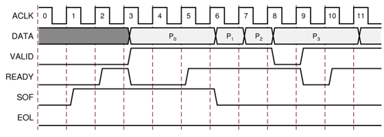
Example of READY/VALID Handshake, Start of a New Frame
AXI4-Stream has additional optional features: sending positional data with TKEEP and TSTRB ports which make it possible to multiplex both data position and data itself on TDATA lines; routing streams by TID and TDIST which roughly corresponds to stream identifier and stream destination identifier 16
6.3 AXI4-Stream Video
AXI4-Stream Video is a subset of AXI4-Stream designed for transporting video frames. AXI4-Stream Video is compatible with AXI4-Stream components, it simply has conventions for the use of ports already defined by AXI4-Stream:
The TLAST signal designates the last pixel of each line, and is also known as end of line (EOL).
The TUSER signal designates the first pixel of a frame and is known as start of frame (SOF).
These two flags are necessary to identify pixel locations on the AXI4 stream interface because there are no sync or blank signals. 17. Video DMA component makes use of the TUSER signal to synchronize frame buffering. Note that TUSER flag which is part of AXI4-Stream specification replaces FSYNC signal that has been used in the past by legacy applications.
7 Video capture with VDMA
7.1 Introduction
The S2MM portion of Video DMA component can be used for video capture.
Ideal pipeline for video capture employing single VDMA instance with only write channel, read channel is disabled.
7.2 Minimal hardware design
As getting everything working at the first attempt is tricky it makes sense to substitute actual camera with test pattern generator and kernel module with a userspace snippet which triggers the DMA transfer.

High level block design for transferring frames from Test Pattern Generator to DDR memory using S2MM portion of single VDMA instance.
Note that in this case there are two clock domains: AXI4-Lite slaves are communicating at 100MHz bus speed, but video signals are transferred at bus frequency of 150MHz. High speed port clock is highlighted with yellow so if you get errors regarding clock domains double check the clock signal routing.

Address mapping with AXI Video Direct Memory Access and AXI Test Pattern Generator
In this case VDMA controller control and status registers are mapped at 0x43000000 using AXI-Lite and that memory address can be written to in order to initiate a DMA transfer. In this example MM2S portion is disabled and S2MM portion of the VDMA controller has access to the whole physical memory range of 512MB on ZYBO via AXI High Performance port. This also bears potential security risk as malicious or buggy FPGA bitstream could make it possible to transmit sensitive DDR memory contents for instance RSA keys to third parties.
Note that without kernel module approach Linux may allocate the DMA memory ranges to applications and that combination may end up with memory corruption. In order to avoid that mem=224M should be added to kernel boot arguments so kernel would not use last 32MB for other processes and threads. Better solution would be of course to implement kernel module which ioremaps DMA memory ranges aswell as control/status register memory ranges.

Test pattern generator 18 is configured to output AXI4-Stream of 24-bit RGB pixels at resolution of 640x480
Such configuration should produce tartan bars pattern.

Tartan bars pattern

Only write channel (stream to memory-mapped) is enabled

s2mm tuser signal emitted by test pattern generator 18 is used for frame synchronization
7.3 Minimal software design
Following example for managing triple-buffered VDMA component should be pretty explainatory. Code is roughtly based on Ales Ruda's work 19 with heavy modifications based on Xilinx reference manual:
/*
 * Triple buffering example for Xilinx VDMA v6.2 IP-core,
 * loosely based on Ales Ruda's work.
 *
 *  Created on: 17.3.2013
 *      Author: Ales Ruda
 *         web: www.arbot.cz
 *
 *  Modified on: 18.12.2014
 *       Author: Lauri Vosandi
 *          web: lauri.vosandi.com
 */

#include <stdio.h>
#include <unistd.h>
#include <fcntl.h>
#include <sys/mman.h>

/* Register offsets */
#define OFFSET_PARK_PTR_REG                     0x28
#define OFFSET_VERSION                          0x2c

#define OFFSET_VDMA_MM2S_CONTROL_REGISTER       0x00
#define OFFSET_VDMA_MM2S_STATUS_REGISTER        0x04
#define OFFSET_VDMA_MM2S_VSIZE                  0x50
#define OFFSET_VDMA_MM2S_HSIZE                  0x54
#define OFFSET_VDMA_MM2S_FRMDLY_STRIDE          0x58
#define OFFSET_VDMA_MM2S_FRAMEBUFFER1           0x5c
#define OFFSET_VDMA_MM2S_FRAMEBUFFER2           0x60
#define OFFSET_VDMA_MM2S_FRAMEBUFFER3           0x64
#define OFFSET_VDMA_MM2S_FRAMEBUFFER4           0x68

#define OFFSET_VDMA_S2MM_CONTROL_REGISTER       0x30
#define OFFSET_VDMA_S2MM_STATUS_REGISTER        0x34
#define OFFSET_VDMA_S2MM_IRQ_MASK               0x3c
#define OFFSET_VDMA_S2MM_REG_INDEX              0x44
#define OFFSET_VDMA_S2MM_VSIZE                  0xa0
#define OFFSET_VDMA_S2MM_HSIZE                  0xa4
#define OFFSET_VDMA_S2MM_FRMDLY_STRIDE          0xa8
#define OFFSET_VDMA_S2MM_FRAMEBUFFER1           0xac
#define OFFSET_VDMA_S2MM_FRAMEBUFFER2           0xb0
#define OFFSET_VDMA_S2MM_FRAMEBUFFER3           0xb4
#define OFFSET_VDMA_S2MM_FRAMEBUFFER4           0xb8

/* S2MM and MM2S control register flags */
#define VDMA_CONTROL_REGISTER_START                     0x00000001
#define VDMA_CONTROL_REGISTER_CIRCULAR_PARK             0x00000002
#define VDMA_CONTROL_REGISTER_RESET                     0x00000004
#define VDMA_CONTROL_REGISTER_GENLOCK_ENABLE            0x00000008
#define VDMA_CONTROL_REGISTER_FrameCntEn                0x00000010
#define VDMA_CONTROL_REGISTER_INTERNAL_GENLOCK          0x00000080
#define VDMA_CONTROL_REGISTER_WrPntr                    0x00000f00
#define VDMA_CONTROL_REGISTER_FrmCtn_IrqEn              0x00001000
#define VDMA_CONTROL_REGISTER_DlyCnt_IrqEn              0x00002000
#define VDMA_CONTROL_REGISTER_ERR_IrqEn                 0x00004000
#define VDMA_CONTROL_REGISTER_Repeat_En                 0x00008000
#define VDMA_CONTROL_REGISTER_InterruptFrameCount       0x00ff0000
#define VDMA_CONTROL_REGISTER_IRQDelayCount             0xff000000

/* S2MM status register */
#define VDMA_STATUS_REGISTER_HALTED                     0x00000001  // Read-only
#define VDMA_STATUS_REGISTER_VDMAInternalError          0x00000010  // Read or write-clear
#define VDMA_STATUS_REGISTER_VDMASlaveError             0x00000020  // Read-only
#define VDMA_STATUS_REGISTER_VDMADecodeError            0x00000040  // Read-only
#define VDMA_STATUS_REGISTER_StartOfFrameEarlyError     0x00000080  // Read-only
#define VDMA_STATUS_REGISTER_EndOfLineEarlyError        0x00000100  // Read-only
#define VDMA_STATUS_REGISTER_StartOfFrameLateError      0x00000800  // Read-only
#define VDMA_STATUS_REGISTER_FrameCountInterrupt        0x00001000  // Read-only
#define VDMA_STATUS_REGISTER_DelayCountInterrupt        0x00002000  // Read-only
#define VDMA_STATUS_REGISTER_ErrorInterrupt             0x00004000  // Read-only
#define VDMA_STATUS_REGISTER_EndOfLineLateError         0x00008000  // Read-only
#define VDMA_STATUS_REGISTER_FrameCount                 0x00ff0000  // Read-only
#define VDMA_STATUS_REGISTER_DelayCount                 0xff000000  // Read-only

typedef struct {
    unsigned int baseAddr;
    int vdmaHandler;
    int width;
    int height;
    int pixelLength;
    int fbLength;
    unsigned int* vdmaVirtualAddress;
    unsigned char* fb1VirtualAddress;
    unsigned char* fb1PhysicalAddress;
    unsigned char* fb2VirtualAddress;
    unsigned char* fb2PhysicalAddress;
    unsigned char* fb3VirtualAddress;
    unsigned char* fb3PhysicalAddress;

    pthread_mutex_t lock;
} vdma_handle;


int vdma_setup(vdma_handle *handle, unsigned int baseAddr, int width, int height, int pixelLength, unsigned int fb1Addr, unsigned int fb2Addr, unsigned int fb3Addr) {
    handle->baseAddr=baseAddr;
    handle->width=width;
    handle->height=height;
    handle->pixelLength=pixelLength;
    handle->fbLength=pixelLength*width*height;
    handle->vdmaHandler = open("/dev/mem", O_RDWR | O_SYNC);
    handle->vdmaVirtualAddress = (unsigned int*)mmap(NULL, 65535, PROT_READ | PROT_WRITE, MAP_SHARED, handle->vdmaHandler, (off_t)handle->baseAddr);
    if(handle->vdmaVirtualAddress == MAP_FAILED) {
        perror("vdmaVirtualAddress mapping for absolute memory access failed.\n");
        return -1;
    }

    handle->fb1PhysicalAddress = fb1Addr;
    handle->fb1VirtualAddress = (unsigned char*)mmap(NULL, handle->fbLength, PROT_READ | PROT_WRITE, MAP_SHARED, handle->vdmaHandler, (off_t)fb1Addr);
    if(handle->fb1VirtualAddress == MAP_FAILED) {
        perror("fb1VirtualAddress mapping for absolute memory access failed.\n");
        return -2;
    }

    handle->fb2PhysicalAddress = fb2Addr;
    handle->fb2VirtualAddress = (unsigned char*)mmap(NULL, handle->fbLength, PROT_READ | PROT_WRITE, MAP_SHARED, handle->vdmaHandler, (off_t)fb2Addr);
    if(handle->fb2VirtualAddress == MAP_FAILED) {
        perror("fb2VirtualAddress mapping for absolute memory access failed.\n");
        return -3;
    }

    handle->fb3PhysicalAddress = fb3Addr;
    handle->fb3VirtualAddress = (unsigned char*)mmap(NULL, handle->fbLength, PROT_READ | PROT_WRITE, MAP_SHARED, handle->vdmaHandler, (off_t)fb3Addr);
    if(handle->fb3VirtualAddress == MAP_FAILED)
    {
     perror("fb3VirtualAddress mapping for absolute memory access failed.\n");
     return -3;
    }

    memset(handle->fb1VirtualAddress, 255, handle->width*handle->height*handle->pixelLength);
    memset(handle->fb2VirtualAddress, 255, handle->width*handle->height*handle->pixelLength);
    memset(handle->fb3VirtualAddress, 255, handle->width*handle->height*handle->pixelLength);
    return 0;
}


void vdma_halt(vdma_handle *handle) {
    vdma_set(handle, OFFSET_VDMA_S2MM_CONTROL_REGISTER, VDMA_CONTROL_REGISTER_RESET);
    vdma_set(handle, OFFSET_VDMA_MM2S_CONTROL_REGISTER, VDMA_CONTROL_REGISTER_RESET);
    munmap((void *)handle->vdmaVirtualAddress, 65535);
    munmap((void *)handle->fb1VirtualAddress, handle->fbLength);
    munmap((void *)handle->fb2VirtualAddress, handle->fbLength);
    munmap((void *)handle->fb3VirtualAddress, handle->fbLength);
    close(handle->vdmaHandler);
}

unsigned int vdma_get(vdma_handle *handle, int num) {
    return handle->vdmaVirtualAddress[num>>2];
}

void vdma_set(vdma_handle *handle, int num, unsigned int val) {
    handle->vdmaVirtualAddress[num>>2]=val;
}

void vdma_status_dump(int status) {
    if (status & VDMA_STATUS_REGISTER_HALTED) printf(" halted"); else printf("running");
    if (status & VDMA_STATUS_REGISTER_VDMAInternalError) printf(" vdma-internal-error");
    if (status & VDMA_STATUS_REGISTER_VDMASlaveError) printf(" vdma-slave-error");
    if (status & VDMA_STATUS_REGISTER_VDMADecodeError) printf(" vdma-decode-error");
    if (status & VDMA_STATUS_REGISTER_StartOfFrameEarlyError) printf(" start-of-frame-early-error");
    if (status & VDMA_STATUS_REGISTER_EndOfLineEarlyError) printf(" end-of-line-early-error");
    if (status & VDMA_STATUS_REGISTER_StartOfFrameLateError) printf(" start-of-frame-late-error");
    if (status & VDMA_STATUS_REGISTER_FrameCountInterrupt) printf(" frame-count-interrupt");
    if (status & VDMA_STATUS_REGISTER_DelayCountInterrupt) printf(" delay-count-interrupt");
    if (status & VDMA_STATUS_REGISTER_ErrorInterrupt) printf(" error-interrupt");
    if (status & VDMA_STATUS_REGISTER_EndOfLineLateError) printf(" end-of-line-late-error");
    printf(" frame-count:%d", (status & VDMA_STATUS_REGISTER_FrameCount) >> 16);
    printf(" delay-count:%d", (status & VDMA_STATUS_REGISTER_DelayCount) >> 24);
    printf("\n");
}

void vdma_s2mm_status_dump(vdma_handle *handle) {
    int status = vdma_get(handle, OFFSET_VDMA_S2MM_STATUS_REGISTER);
    printf("S2MM status register (%08x):", status);
    vdma_status_dump(status);
}

void vdma_mm2s_status_dump(vdma_handle *handle) {
    int status = vdma_get(handle, OFFSET_VDMA_MM2S_STATUS_REGISTER);
    printf("MM2S status register (%08x):", status);
    vdma_status_dump(status);
}

void vdma_start_triple_buffering(vdma_handle *handle) {
    // Reset VDMA
    vdma_set(handle, OFFSET_VDMA_S2MM_CONTROL_REGISTER, VDMA_CONTROL_REGISTER_RESET);
    vdma_set(handle, OFFSET_VDMA_MM2S_CONTROL_REGISTER, VDMA_CONTROL_REGISTER_RESET);

    // Wait for reset to finish
    while((vdma_get(handle, OFFSET_VDMA_S2MM_CONTROL_REGISTER) & VDMA_CONTROL_REGISTER_RESET)==4);
    while((vdma_get(handle, OFFSET_VDMA_MM2S_CONTROL_REGISTER) & VDMA_CONTROL_REGISTER_RESET)==4);

    // Clear all error bits in status register
    vdma_set(handle, OFFSET_VDMA_S2MM_STATUS_REGISTER, 0);
    vdma_set(handle, OFFSET_VDMA_MM2S_STATUS_REGISTER, 0);

    // Do not mask interrupts
    vdma_set(handle, OFFSET_VDMA_S2MM_IRQ_MASK, 0xf);

    int interrupt_frame_count = 3;

    // Start both S2MM and MM2S in triple buffering mode
    vdma_set(handle, OFFSET_VDMA_S2MM_CONTROL_REGISTER,
        (interrupt_frame_count << 16) |
        VDMA_CONTROL_REGISTER_START |
        VDMA_CONTROL_REGISTER_GENLOCK_ENABLE |
        VDMA_CONTROL_REGISTER_INTERNAL_GENLOCK |
        VDMA_CONTROL_REGISTER_CIRCULAR_PARK);
    vdma_set(handle, OFFSET_VDMA_MM2S_CONTROL_REGISTER,
        (interrupt_frame_count << 16) |
        VDMA_CONTROL_REGISTER_START |
        VDMA_CONTROL_REGISTER_GENLOCK_ENABLE |
        VDMA_CONTROL_REGISTER_INTERNAL_GENLOCK |
        VDMA_CONTROL_REGISTER_CIRCULAR_PARK);


    while((vdma_get(handle, 0x30)&1)==0 || (vdma_get(handle, 0x34)&1)==1) {
        printf("Waiting for VDMA to start running...\n");
        sleep(1);
    }

    // Extra register index, use first 16 frame pointer registers
    vdma_set(handle, OFFSET_VDMA_S2MM_REG_INDEX, 0);

    // Write physical addresses to control register
    vdma_set(handle, OFFSET_VDMA_S2MM_FRAMEBUFFER1, handle->fb1PhysicalAddress);
    vdma_set(handle, OFFSET_VDMA_MM2S_FRAMEBUFFER1, handle->fb1PhysicalAddress);
    vdma_set(handle, OFFSET_VDMA_S2MM_FRAMEBUFFER2, handle->fb2PhysicalAddress);
    vdma_set(handle, OFFSET_VDMA_MM2S_FRAMEBUFFER2, handle->fb2PhysicalAddress);
    vdma_set(handle, OFFSET_VDMA_S2MM_FRAMEBUFFER3, handle->fb3PhysicalAddress);
    vdma_set(handle, OFFSET_VDMA_MM2S_FRAMEBUFFER3, handle->fb3PhysicalAddress);

    // Write Park pointer register
    vdma_set(handle, OFFSET_PARK_PTR_REG, 0);

    // Frame delay and stride (bytes)
    vdma_set(handle, OFFSET_VDMA_S2MM_FRMDLY_STRIDE, handle->width*handle->pixelLength);
    vdma_set(handle, OFFSET_VDMA_MM2S_FRMDLY_STRIDE, handle->width*handle->pixelLength);

    // Write horizontal size (bytes)
    vdma_set(handle, OFFSET_VDMA_S2MM_HSIZE, handle->width*handle->pixelLength);
    vdma_set(handle, OFFSET_VDMA_MM2S_HSIZE, handle->width*handle->pixelLength);

    // Write vertical size (lines), this actually starts the transfer
    vdma_set(handle, OFFSET_VDMA_S2MM_VSIZE, handle->height);
    vdma_set(handle, OFFSET_VDMA_MM2S_VSIZE, handle->height);
}

int vdma_running(vdma_handle *handle) {
    // Check whether VDMA is running, that is ready to start transfers
    return (vdma_get(handle, 0x34)&1)==1;
}

int vdma_idle(vdma_handle *handle) {
    // Check whtether VDMA is transferring
    return (vdma_get(handle, OFFSET_VDMA_S2MM_STATUS_REGISTER) & VDMA_STATUS_REGISTER_FrameCountInterrupt)!=0;
}

int main() {
    int j, i;
    vdma_handle handle;

    // Setup VDMA handle and memory-mapped ranges
    vdma_setup(&handle, 0x43000000, 640, 480, 4, 0x0e000000, 0x0f000000, 0x10000000);

    // Start triple buffering
    vdma_start_triple_buffering(&handle);

    // Run for 10 seconds, just monitor status registers
    for(i=0; i<10; i++) {
        vdma_s2mm_status_dump(&handle);
        vdma_mm2s_status_dump(&handle);
        printf("FB1:\n");
        for (j = 0; j < 256; j++) printf(" %02x", handle.fb1VirtualAddress[j]); printf("\n");
        sleep(1);
    }

    // Halt VDMA and unmap memory ranges
    vdma_halt(&handle);
}
Note that this is just a demo code which is not exactly usable for any practical application mainly because the memory ranges assigned for framebuffers are not reserved by any kernel module. For real applications AXI (V)DMA driver should be used. It builds proper abstraction such as /dev/axi_dma_0 or /dev/axi_vdma_0 which can be accessed from userspace applications 20.
7.4 Grabbing frames over HTTP
Once the VDMA transfer is running you can use following Python snippet on the ZYBO to grab a frame from DDR memory and serve it over HTTP:
import os, png, mmap, BaseHTTPServer

FRAMEBUFFER_OFFSET=0x0e000000
WIDTH = 640
HEIGHT = 480
PIXEL_SIZE = 4

fh = os.open("/dev/mem", os.O_SYNC | os.O_RDONLY) # Disable cache, read-only
mm = mmap.mmap(fh, WIDTH*HEIGHT*PIXEL_SIZE, mmap.MAP_SHARED, mmap.PROT_READ, offset=FRAMEBUFFER_OFFSET)
class MyHandler(BaseHTTPServer.BaseHTTPRequestHandler):
    def do_GET(s):
        writer = png.Writer(WIDTH, HEIGHT, alpha=True)
        s.send_response(200)
        s.send_header("Content-type", "image/png")
        s.end_headers()
        writer.write_array(s.wfile,[ord(j) for j in mm[0:WIDTH*HEIGHT*PIXEL_SIZE]] )

httpd = BaseHTTPServer.HTTPServer(("0.0.0.0", 80), MyHandler)
try:
    httpd.serve_forever()
except KeyboardInterrupt:
    pass
httpd.server_close()

mm.close()
fh.close()
Simply open http://zybo-ip-address:80 on your laptop assuming that the laptop and ZYBO are attached to same network.
7.5 Interfacing with OV7670 camera module
The Hamsterworks controller block can be reused to initialize the camera, there are no modifications required there. The Hamsterworks capture component however is not suitable for interfacing with AXI4-Stream Video compatible cores. Thus we need a slightly modified block which generates corresponding frame and line synchronization primitives.
----------------------------------------------------------------------------------
-- Authors: Mike Field <hamster@snap.net.nz>
--          Lauir Vosandi <lauri.vosandi@gmail.com>
----------------------------------------------------------------------------------
library ieee;
use ieee.std_logic_1164.all;
use ieee.numeric_std.all;

entity ov7670_axi_stream_capture is
    port (
        pclk              : in  std_logic;
        vsync             : in  std_logic;
        href              : in  std_logic;
        d                 : in  std_logic_vector (7 downto 0);
        m_axis_tvalid     : out std_logic;
        m_axis_tready     : in  std_logic;
        m_axis_tlast      : out std_logic;
        m_axis_tdata      : out std_logic_vector ( 31 downto 0 );
        m_axis_tuser      : out std_logic;
        aclk              : out std_logic
    );
end ov7670_axi_stream_capture;

architecture behavioral of ov7670_axi_stream_capture is
    signal d_latch          : std_logic_vector(15 downto 0) := (others => '0');
    signal address          : std_logic_vector(18 downto 0) := (others => '0');
    signal line             : std_logic_vector(1 downto 0)  := (others => '0');
    signal href_last        : std_logic_vector(6 downto 0)  := (others => '0');
    signal we_reg           : std_logic := '0';
    signal href_hold        : std_logic := '0';
    signal latched_vsync    : std_logic := '0';
    signal latched_href     : std_logic := '0';
    signal latched_d        : std_logic_vector (7 downto 0) := (others => '0');
    signal sof              : std_logic := '0';
    signal eol              : std_logic := '0';
begin
     -- Expand 16-bit RGB (5:6:5) to 32-bit RGBA (8:8:8:8)
     m_axis_tdata  <= "11111111"  & d_latch(4 downto 0) & d_latch(0) & d_latch(0) & d_latch(0) & d_latch(10 downto 5) & d_latch(5) & d_latch(5) & d_latch(15 downto 11) & d_latch(11) & d_latch(11) & d_latch(11);
     m_axis_tvalid <= we_reg;
     m_axis_tlast <= eol;
     m_axis_tuser <= sof;
     aclk <= not pclk;

capture_process: process(pclk)
begin
    if rising_edge(pclk) then
        if we_reg = '1' then
            address <= std_logic_vector(unsigned(address)+1);
        end if;

        if href_hold = '0' and latched_href = '1' then
            case line is
                when "00" => line <= "01";
                when "01" => line <= "10";
                when "10" => line <= "11";
                when others => line <= "00";
            end case;
        end if;
        href_hold <= latched_href;

        -- Capturing the data from the camera
        if latched_href = '1' then
            d_latch <= d_latch( 7 downto 0) & latched_d;
        end if;
        we_reg  <= '0';

        -- Is a new screen about to start (i.e. we have to restart capturing)
        if latched_vsync = '1' then
            address        <= (others => '0');
            href_last     <= (others => '0');
            line            <= (others => '0');
        else
            -- If not, set the write enable whenever we need to capture a pixel
            if href_last(0) = '1' then
                we_reg <= '1';
                href_last <= (others => '0');
            else
                href_last <= href_last(href_last'high-1 downto 0) & latched_href;
            end if;
        end if;

        case unsigned(address) mod 640 = 639 is
            when true => eol <= '1';
            when others => eol <= '0';
        end case;

        case unsigned(address) = 0 is
            when true => sof <= '1';
            when others => sof <= '0';
        end case;
    end if;
    if falling_edge(pclk) then
        latched_d     <= d;
        latched_href  <= href;
        latched_vsync <= vsync;
    end if;
end process;
end behavioral;
Modified block converts 16-bit RGB (5:6:5) signal to 32-bit RGBA (8:8:8:8) signal with fake opaque alpha channel. This way whole pixel is transferred during one AXI bus cycle and start-of-frame and end-of-line signals are perfectly aliged with the content.
Substituting test pattern generator with the modified capture block and adding controller block should be enough to have the video input from the camera connected to AXI4-Stream Video compatible pipeline.
7.6 Video4Linux2 driver
As Zynq-7000 boards have I²C bus master built-in, it make sense to take advantage of that feature instead of implementing controller block from scratch. On ZYBO the EEPROM and audio codec are connected to the I²C bus, but it should be possible to route I²C bus to Pmod connectors using IIC_0 port on Zynq7 processing system block. It should also be possible to access the I²C bus via /dev/i2c-0 device node if corresponding kernel modules have been loaded 22. This should make it possible to take advantage of OV7670 kernel module 23 which was written for One Laptop Per Child project. This way the camera initialization can be done by kernel and the camera can be configured via any Video4Linux application instead of static bitstream. How transferring the frames could be done in this case is not however clear yet.
8 Complete video processing pipeline on ZYBO
8.1 Introduction
Xilinx libraries contain Video Direct Memory Access (VDMA) IP-core which can be used to transfer AXI4-Stream protocol based video stream to DDR memory and vice versa. Corresponding sub-components are S2MM (Stream to memory-mapped) also known as write channel and MM2S (Memory-mapped to stream) also known as read channel. Using both of them a video buffer can be implemented with optional crop and zoom features 24.
8.2 Minimal hardware design
This is the last and the most complex example of what I have tried on the ZYBO.
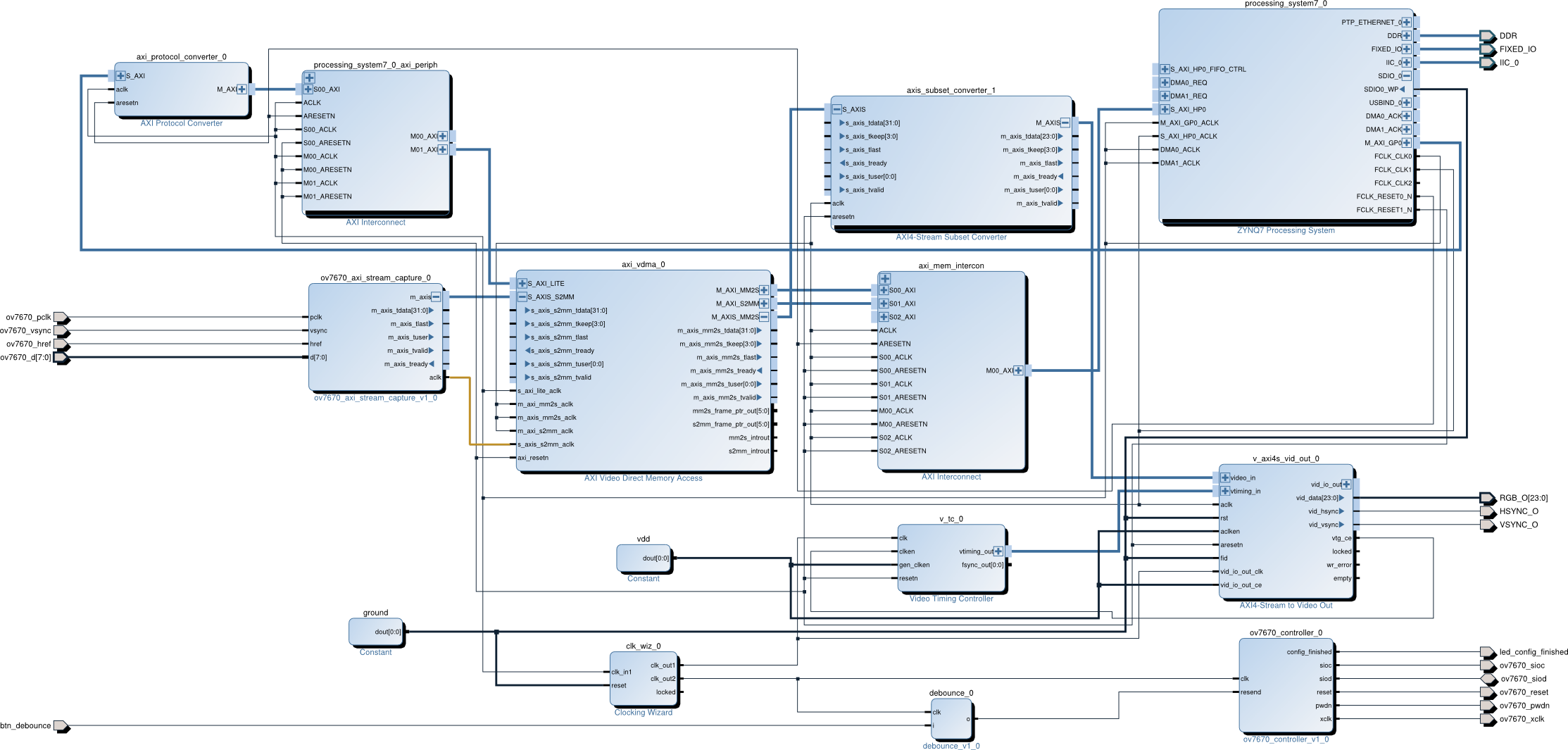
High level block design for complete hardware pipeline
In this example we connect Omnivision OV7670 camera via modified capture block to AXI4-Stream Video compatible pipeline. The VDMA controller maintains a ring buffer in the DDR memory and transfers the frame data to these buffers as the frames are received by S2MM portion of the VDMA controller.
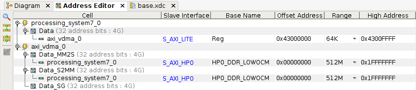
Address mapping with AXI Video Direct Memory Access
8.3 Conclusion
If you've followed the guide you should know by now more or less how the video streams are handled on Zynq-7000 based boards. If that's not the case then I have failed. The code snippets can be found at GitHub repository 26. Most up to date VHDL and Zynq-7000 materials can be found on Lauri's blog 27.