KiCad24. May '17
Introduction
KiCad is open source electronic design automation tool with a long history starting from 1992. CERN started supporting the project since 2013 which has contributed to the maturity of the project considerably.
KiCad distinctly separates logical design and physical design. First the electrical circuits are described with symbols. Then footprints are associated with the components. Footprints are then laid out on the PCB:
Schematic design
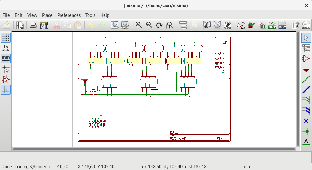
Eeschema is the schematic design tool of KiCad
Some important default keyboard shortcuts:
M - Move component without affecting surrounding objects
G - Grab component while keeping wires intact
X - Flip component along X axis
Y - Flip component along Y axis
R - Rotate component
W - Insert wire
Del - Remove track object
F1 and F2 - Zoom in and out
V - Change value of component
Assigning footprints
From Eeschema main menu select Tools -> Assign Component Footprint, this will open up Cvpcb. From the Cvpcb toolbar disable filtering footprints by keywords and enable filtering by pin count and library. Select categroy from leftmost panel, click on the middle panel to select target component and double click in the rightmost panel to assign a footprint.
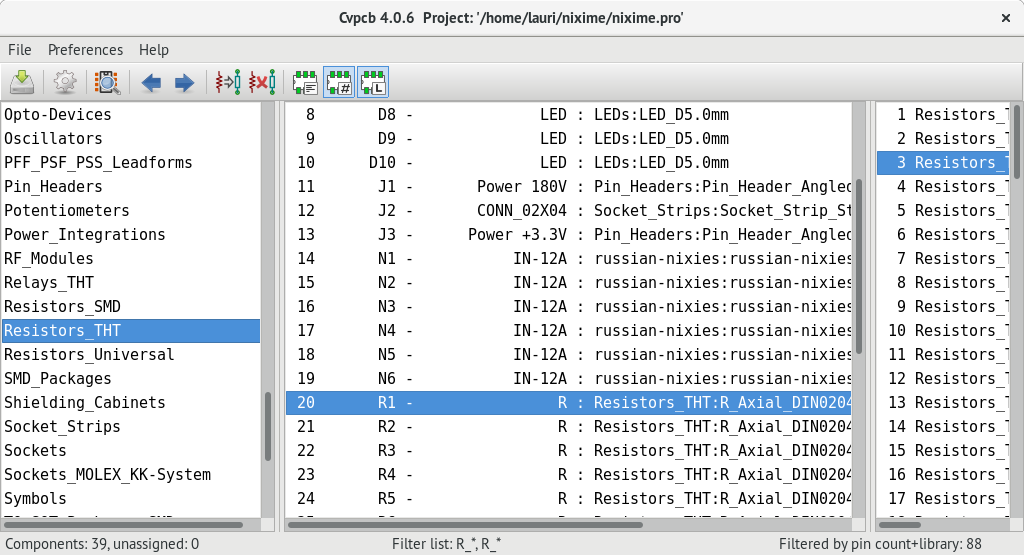
Cvpcb is used to associate schematic components with footprints
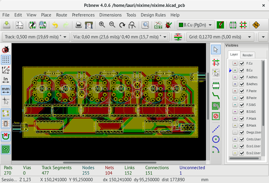
Laying out PCB
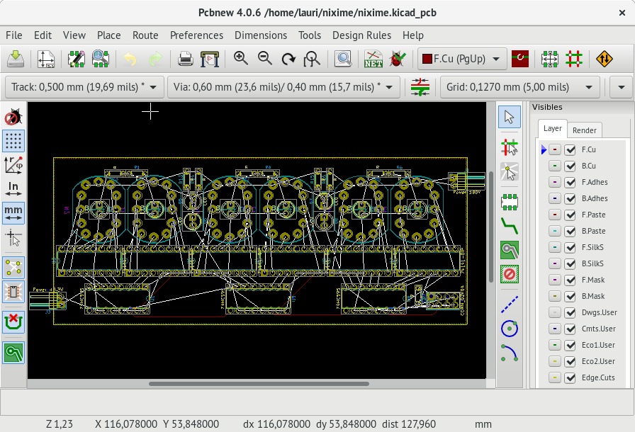
Pcbnew is the PCB layout tool of KiCad
Some important default keyboard shortcuts:
M - Move footprint without affecting surrounding objects
G - Grab footprint while keeping tracks intact
F - Flip a footprit to the other side of PCB
R - Rotate footprint
X - Insert track
Del - Remove track object
F1 and F2 - Zoom in and out
Alt-3 - Open 3D viewer
V - Swap layers, while inserting a track places via
On the status bar Pcbnew shows absolute coordinates and also relative ones. The relative coordinates are measured to point set by pressing the spacebar. This comes very handy in ensuring that you place footprints correctly.
Once tracks have been placed it's time to specify cutout area for the PCB. This will define the dimensions of your PCB. Select Edge.Cuts layer from the layers combobox. From the toolbar select Add graphic line or polygon and draw the rectangle around your design. Hit V to go back to copper layers.
It's possible to fill in rest of the PCB with copper areas usually connected to ground. This reduces the amount of solvent required when etching PCB-s later on. From the main menu select Place -> Zone, click on the cutout corner and select GND as the net where zone shall be connected to. Follow the corners of the cutout and doule click on the corner where you started. Hit V to select the other copper layer and repeat the zone add procedure again. Once both zones have been placed hit B to fill in the zones. Filled zones make it harder to work with footprints, use Ctrl-B to clear zones for the time being.
Autorouting
KiCad doesn't include tool for automatic routing, instead integration with FreeRoute tool is provided. From the main menu select Tools -> FreeRoute, in the toolbar in can be found by yellow icon. In the dialog hit Export a Specctra Design and Launch FreeRoute. Your PCB layout is exported to a .dsn file and opened with FreeRoute. FreeRoute is a Java program so appropriate Java Runtime might have to be additionally installed.
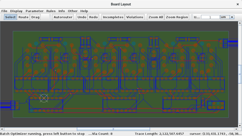
In FreeRouter click Autorouter button on the top, FreeRouting will do it's magic and stop when ready. Note that in certain corner cases it might get stuck between two possible outcomes and you might have to stop the autorouting process manually. Click File -> Export Specctra Session File in the FreeRouting main menu to export .ses file. Now in Pcbnew click Back import the Specctra Session. Press B to refill zones.
If you want FreeRouter to use wider tracks make necessary changes by opening Design Rules from Pcbnew main menu, repeat the export .dsn process and reopen file with FreeRoute. Note that it's perfectly okay to manually route some tracks before running FreeRoute.
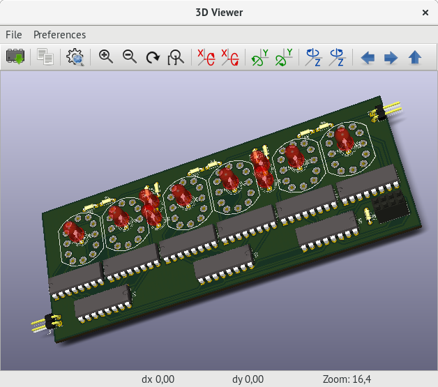
3D view
In KiCad PCB layout editor press Alt-3 to open 3D viewer of the PCB. From the 3D viewer Preferences menu enable Realistic Mode, disable axes, hide grid and under Render Options enable everything.
Gerber export
Once PCB is laid out in KiCad, it can be converted to Gerber. Gerber files basically describe polygons that need to be carved out of the copper layer. You can use gerbview to view Gerber files, command to view all relevant files in current directory:
gerbview *.g*If the Gerbers look alright you can upload them to PCB manufacturing company such as OSH Park, DirtyPCBs, Seeed Studio or probably many others you can find on the internet. Note that for cheap options the shipping time can be anywhere between 1 to 2 months.
Alternatively you can use a CNC machine to mill a PCB.